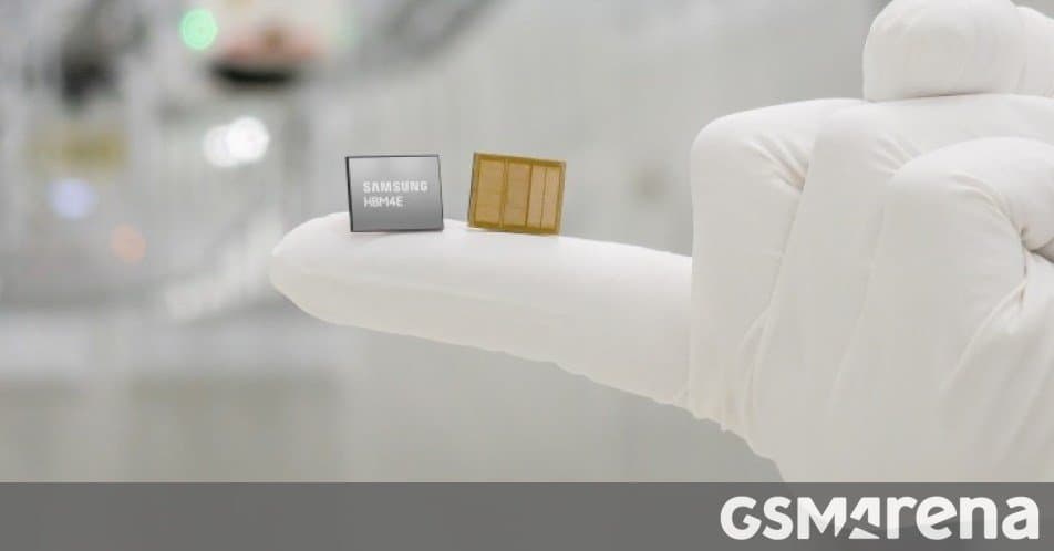
Samsung has started delivering HBM4E memory samples to customers, boosting per‑pin bandwidth to 14 Gbps, raising stack capacity to 48 GB and cutting power use by 16 %. The move expands Samsung’s AI‑focused memory portfolio and hints at future speed upgrades.
Samsung Begins Shipping HBM4E Samples – Faster, Cooler, Higher‑Capacity AI Memory
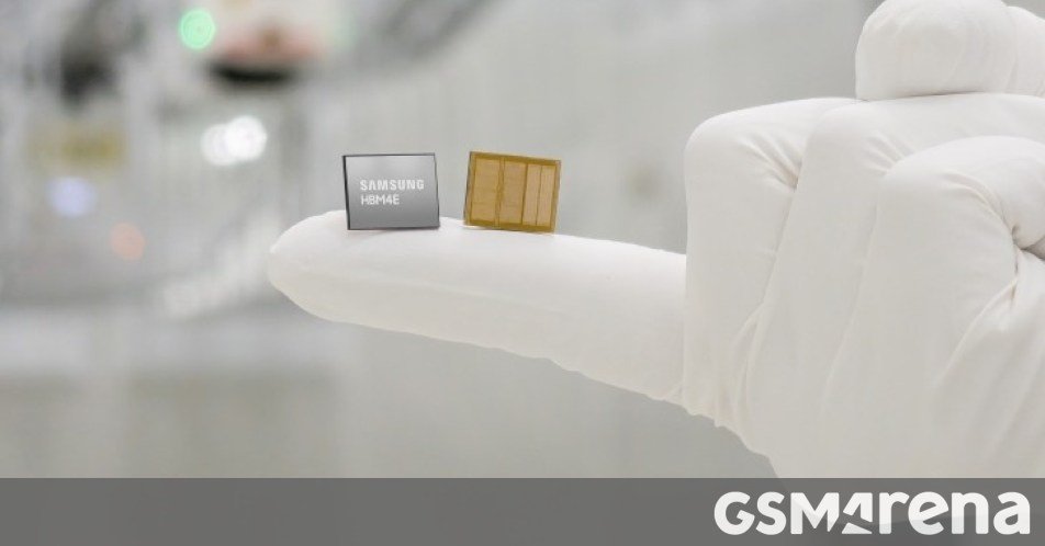
Samsung’s memory division announced that it is now shipping samples of its next‑generation HBM4E (High‑Bandwidth Memory) to select customers. The timing lines up with the company’s promise earlier this year to deliver an upgraded version of HBM4 later in 2026. While the original HBM4 already set a high bar for AI‑centric workloads, HBM4E pushes the envelope further with more capacity, higher per‑pin speeds and notable efficiency gains.
Key specifications and performance gains
| Feature | HBM4 | HBM4E |
|---|---|---|
| Die stack configuration | 12‑layer (36 GB) | 12‑layer (48 GB) |
| Per‑pin data rate | 11.7 Gbps | 14 Gbps (+20 %) |
| Stack bandwidth | 3.6 TB/s | 3.6 TB/s (same aggregate, higher per‑pin) |
| Power efficiency | Baseline | –16 % power, –14 % thermal resistance |
| Process nodes | 10 nm class “1c” memory die + 4 nm logic base | Same nodes, re‑engineered layout |
The 12‑layer stack now holds 48 GB, a 33 % jump over the 36 GB HBM4 stack. Samsung also disclosed plans for an 8‑layer 32 GB variant and a 16‑layer 64 GB version, giving system designers a broader set of options for building AI accelerators, graphics cards and high‑performance compute nodes.
Bandwidth and speed
HBM4E’s per‑pin speed of 14 Gbps translates to a raw data rate of 3.6 TB/s per stack—identical to HBM4’s total bandwidth but achieved with fewer pins operating faster. This higher pin speed reduces the number of required I/O connections, simplifying PCB routing for dense server boards. Samsung has hinted that the 14 Gbps figure is a stepping stone; the design can be pushed to 16 Gbps in future revisions without a major redesign.
Power and thermal improvements
By moving to a refined 4 nm logic base die and optimizing the interposer layout, Samsung reports a 16 % reduction in power consumption and a 14 % drop in thermal resistance. In practical terms, a typical AI accelerator using a 48 GB HBM4E stack will run cooler and draw less power than an equivalent HBM4 configuration, easing cooling requirements and potentially allowing higher clock speeds or denser packaging.
Ecosystem impact and why it matters for AI hardware
AI data‑center acceleration
High‑bandwidth memory is a critical bottleneck for large language models and other deep‑learning workloads that need to move terabytes of data per second between compute cores and memory. Samsung’s HBM4E directly addresses that bottleneck, offering more capacity per stack, which means fewer stacks are needed to reach a given memory footprint. Fewer stacks reduce board complexity and can lower overall system cost.
Competition and supply chain considerations
AMD recently announced a multi‑year supply agreement with Samsung for HBM4, positioning the company as a key supplier for next‑gen GPUs and AI ASICs. With HBM4E samples now in the hands of early adopters, Samsung is likely to secure follow‑on contracts for the higher‑capacity variants, potentially shifting market share away from competing HBM providers such as SK Hynix and Micron.
Design flexibility for OEMs
The announced 32 GB (8‑layer) and 64 GB (16‑layer) options give OEMs the ability to tailor memory configurations to specific product tiers. A mid‑range AI accelerator could opt for the 32 GB stack to keep costs down, while a flagship server might integrate multiple 64 GB stacks for a petabyte‑scale memory pool.
Looking ahead
Samsung’s executive vice‑president for memory development, Sang Joon Hwang, emphasized that the company’s “pre‑emptive infrastructure investments” will keep it at the forefront of the AI memory market. The current HBM4E sample shipment is a proof point that Samsung can move from mass‑production of HBM4 to rapid iteration on the next generation.
Future roadmap items include:
- Scaling the per‑pin rate to 16 Gbps without sacrificing the 12‑layer form factor.
- Expanding the 64 GB 16‑layer stack for ultra‑high‑capacity AI servers.
- Integrating HBM4E with emerging compute‑in‑memory architectures that place logic directly on the memory stack.
For developers and system architects, the practical takeaway is clear: HBM4E offers a tangible path to higher performance AI systems with lower power budgets. Early adopters who can secure samples now will be positioned to ship next‑generation AI hardware ahead of competitors.
References
- Samsung press release on HBM4E sampling (official page)
- AMD‑Samsung HBM4 supply agreement details (AMD blog)
- Technical deep‑dive on HBM architecture (JEDEC documentation)
Comments
Please log in or register to join the discussion