TSMC is advancing its System on Integrated Chips (SoIC) 3D stacking technology, evolving from face-to-back to face-to-face stacking, with pitch sizes expected to shrink from 6 microns today to 4.5 microns by 2029. This advancement will enable higher bandwidth, lower latency, and improved energy efficiency for next-generation AI and HPC processors, as demonstrated in Fujitsu's upcoming Monaka supercomputer CPU.
TSMC's chip-on-wafer-on-substrate (CoWoS) packaging technology has become the industry standard for advanced AI and HPC processors using HBM memory. However, the company's vertically integrated System on Integrated Chips (SoIC) technology with 3D interconnects has not seen as widespread adoption—until now. At its recent North American Technology Symposium, TSMC outlined an aggressive development path for SoIC technology that will transform how advanced processors are designed and manufactured.
The Evolution of 3D Stacking
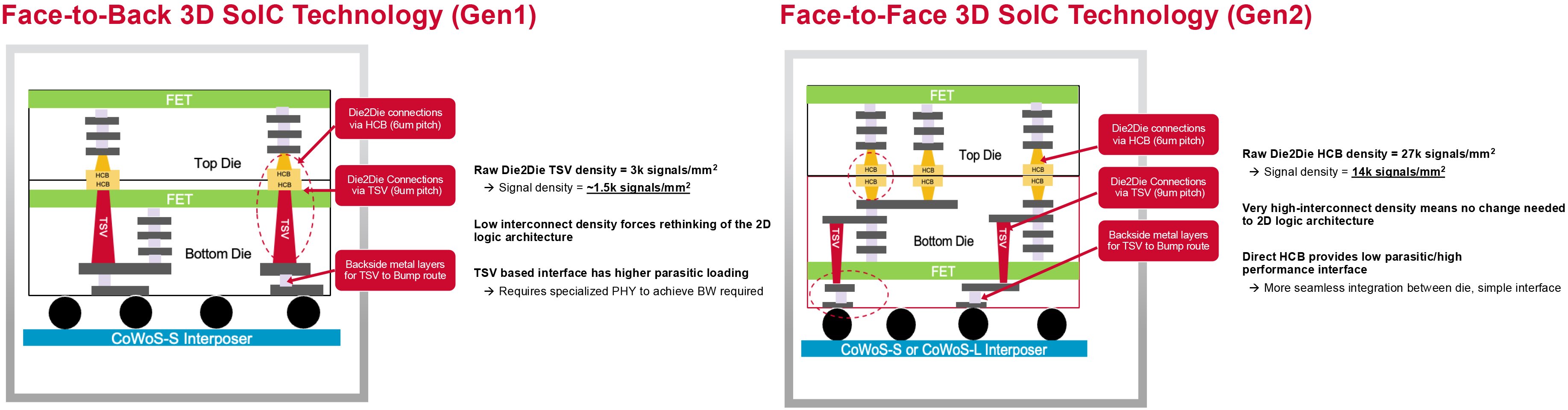
TSMC's SoIC technology has historically played second fiddle to CoWoS, with slower adoption of new process technologies. In 2023, the first generation offered a 9-micron interconnection pitch, sufficient for products like AMD's Instinct MI300-series. However, this initial implementation had a critical limitation: it only supported face-to-back (F2B) stacking, not the more advanced face-to-face (F2F) stacking enabled by the second generation.
The fundamental constraint of F2B stacking lies in its signal routing. Signals cannot travel directly between dies; instead, they must traverse multiple metal layers and pass through silicon vias (TSVs) in the bottom die. This indirect path increases latency, power consumption, and routing complexity. According to Broadcom, a real-world F2B design can achieve approximately 1,500 signals per square millimeter with TSVs.
Face-to-face stacking eliminates this limitation by aligning the metal layers of two dies directly and connecting them using hybrid copper bonding. This approach enables straight, ultra-short vertical interconnects without relying on TSVs, increasing signal density by an order of magnitude to 14,000 signals per square millimeter. The result is significantly higher bandwidth, reduced latency, and lower energy consumption per bit of data transferred.
The performance benefits are substantial enough that companies like Broadcom consider F2F stacking crucial for scaling compute density in next-generation AI and HPC processors. The communication between stacked dies effectively resembles on-die wiring rather than traditional chip-to-chip links.
TSMC's Technical Roadmap
With both F2F and F2B stacking now available, TSMC's development of SoIC technology will accelerate significantly. The company has outlined a clear progression of process node combinations:
- Current: N3P dies on top of N4 dies
- Near-term: N2P on top of N3P within the next year
- Mid-term: N2P on top of N2P by 2028
- Long-term: 3D stacked A14 dies by 2029
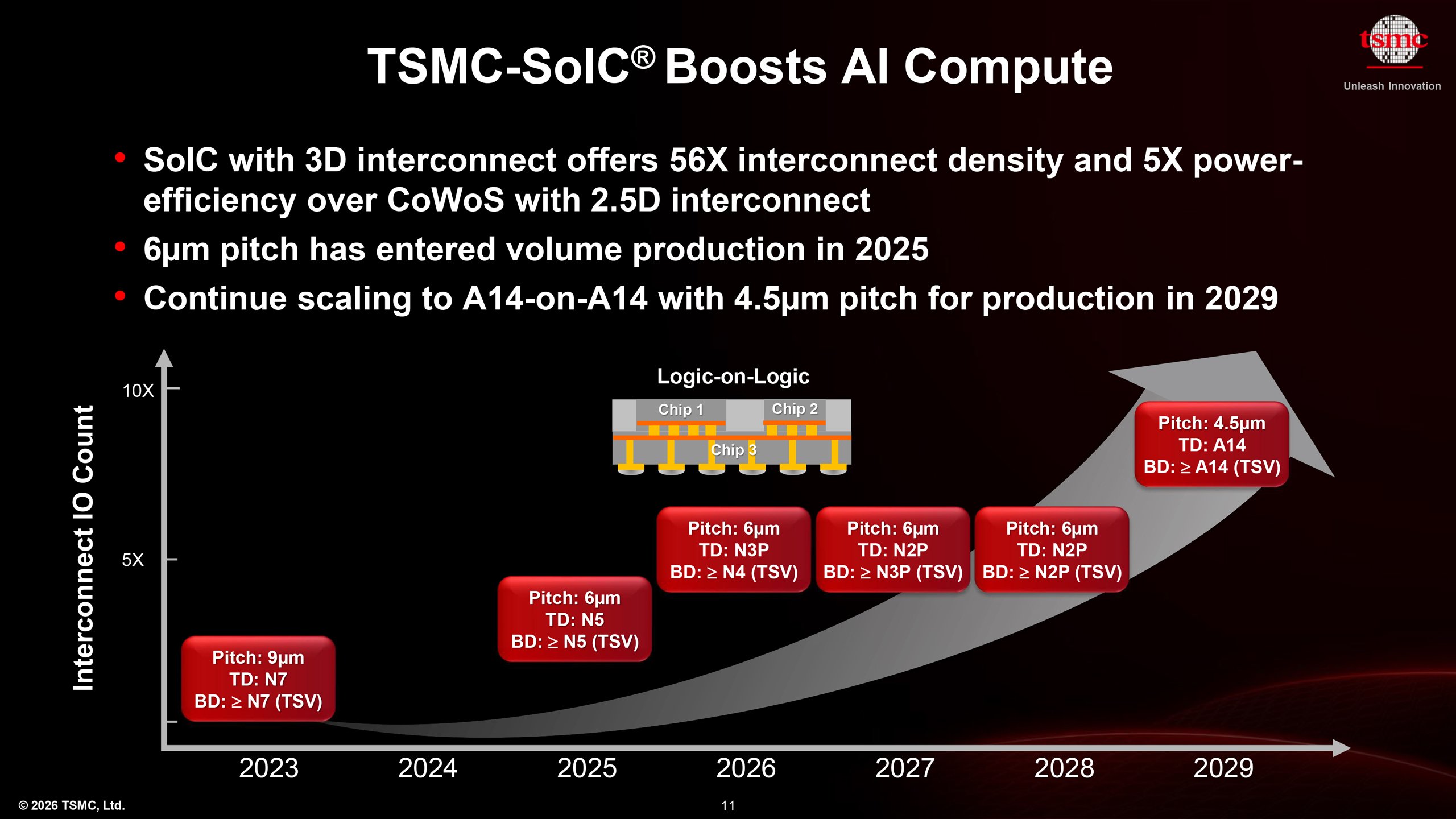
The roadmap also details aggressive pitch scaling, from 9 microns in 2023 to 6 microns achieved in 2025, with a target of 4.5 microns by 2029. This reduction in pitch size enables even higher interconnection density and performance.
Notably, the presented roadmap doesn't include backside power delivery for these nodes. However, TSMC Senior Vice President Kevin Zhang clarified that this omission was for simplicity and that A16 will indeed support stacking capabilities. "The SoIC roadmap shown does not cover all possible combinations—there are many permutations," Zhang explained. "The key takeaways are twofold. First, pitch scaling—from 9 µm to 6 µm, and eventually down to 4.5 µm. Second, the acceleration of stacking timelines."
The acceleration is particularly evident when comparing past and future TSV availability. Previously, 3nm TSV wasn't expected until around 2027. By 2029, however, A14 TSV will be available just one year after initial production, enabling customers to stack the most advanced dies much sooner than previously possible.
Real-World Implementation: Fujitsu's Monaka Supercomputer CPU
As a leading developer of custom processors for hyperscalers, Broadcom has become one of the primary adopters of TSMC's advanced packaging technologies. The company is now implementing TSMC's F2F SoIC technology in Fujitsu's upcoming Monaka supercomputer CPU.
The Monaka processor represents a significant advancement in data center computing, featuring 144 Armv9 cores distributed across four compute chiplets manufactured on TSMC's N2 process. These CPU chiplets are stacked face-to-face atop dedicated SRAM chiplets (built on N5 technology) using hybrid copper bonding. The design also includes a substantial I/O die that integrates the processor's memory controllers and PHYs for 12 DDR5 channels, along with PCIe 6.0 connectivity with CXL 3.0 support for accelerators and memory expanders.
This architecture allows Broadcom and Fujitsu to incorporate massive amounts of cache into the Armv9 cores, maximizing single-thread performance in a cost-effective manner. The trade-off is increased design complexity and thermal management challenges, which is why the current implementation avoids stacking logic-on-logic—a capability that remains under development.
Broadcom is currently sampling Monaka with Fujitsu and plans to begin volume production in 2027. Despite using the more advanced hybrid bonding technology, the implementation still employs 9-micron pitches, indicating that even industry leaders are approaching the latest 3D integration technologies cautiously. This contrasts with CoWoS, where TSMC's clients eagerly adopt the latest versions for bleeding-edge processors.
Market Implications and Future Outlook
TSMC's aggressive SoIC development comes at a critical time when transistor scaling is slowing down. As traditional Moore's Law scaling becomes increasingly difficult and expensive, packaging technologies are emerging as the primary engine for performance improvements. The ability to stack dies with higher interconnect density directly translates to improved compute density and performance per watt.
The adoption of F2F stacking technology will be particularly important for AI and HPC applications, where memory bandwidth and low-latency communication between compute elements are paramount. The order-of-magnitude increase in signal density—from 1,500 to 14,000 signals/mm2—enables architectures that were previously impractical due to interconnection limitations.
As TSMC continues to refine its SoIC technology and reduce pitch sizes, we can expect to see more complex 3D stacking implementations. The eventual adoption of logic-on-logic stacking would enable even more sophisticated processor architectures, potentially combining different process technologies within a single package to optimize performance, power, and cost.
The development of SoIC technology represents a significant step forward in semiconductor packaging, moving beyond simple 2.5D integration to true 3D system integration. As this technology matures and becomes more widely adopted, it will play an increasingly important role in enabling the next generation of high-performance computing systems.
For more information on TSMC's packaging technologies, visit their official packaging solutions page.
Comments
Please log in or register to join the discussion