
A comprehensive exploration of DDR4 SDRAM initialization, training, and calibration processes, explaining the critical steps required to bring DRAM from power-up to operational state.
DDR4 SDRAM Initialization: From Power-Up to Operational State
Introduction
When a device with a DRAM sub-system is powered up, a number of critical processes occur before the DRAM becomes operational. The initialization procedure consists of four distinct phases that transform the DRAM from a powered-off state to a fully functional memory system.
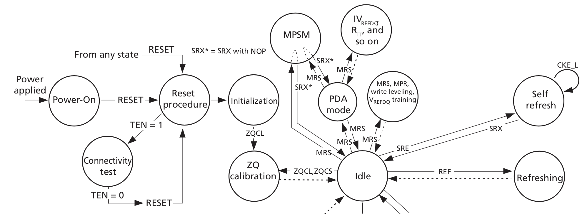 Figure 1: DDR4 State Machine (Source: Micron Datasheet)
The Four Phases of DDR4 Initialization
- Power-up and Initialization
- ZQ Calibration
- Vref DQ Calibration
- Read/Write Training
To better understand these phases, let's consider a typical system with an ASIC/FPGA/Processor connected to a single DIMM module.
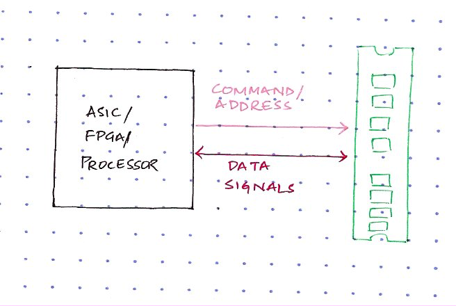 Figure 2: Example System Initialization
Power-up and Initialization
Power-up and initialization is a fixed, well-defined sequence of steps that typically occurs automatically when the system is powered up and the controller is removed from reset. The controller performs the following sequence:
- Apply power to the DRAM
- De-assert RESET and activate ClockEnable (CKE)
- Enable clocks (CK_t/CK_c)
- Issue MRS commands and load Mode Registers in a specific sequence
- Perform ZQ Calibration (ZQCL)
- Bring the DRAM into IDLE state
At this point, the DRAMs understand their operating frequency, CAS Latency (CL), CAS Write Latency (CWL), and other timing parameters.
ZQ Calibration
ZQ Calibration is crucial for data integrity and relates to the data pins (DQ). Each DQ pin is bidirectional, responsible for sending data during reads and receiving data during writes.
 Figure 4: ZQCL (Source: Micron Datasheet)
Why ZQ Calibration is Required
The circuit behind each DQ pin consists of parallel 240Ω resistor legs. Due to the nature of CMOS devices, these resistors are never exactly 240Ω and are affected by voltage and temperature changes. To address this, each DRAM has a DQ calibration control block and a ZQ pin connected to an external precision 240Ω resistor.
When a ZQCL command is issued during initialization, the DQ calibration control block produces a tuning value that is copied to each DQ's internal circuitry, ensuring precise resistance values.
Technical Details
The 240Ω resistor leg uses a "Poly Silicon Resistor" that is slightly larger than 240Ω. Multiple p-channel devices are connected in parallel to allow precise tuning. The calibration process involves a resistor divider circuit with a comparator that tunes the p-channel devices until the voltage is exactly VDDq/2.
This calibration capability allows control over drive strength (for reads) and termination resistance (for writes), improving signal integrity and allowing high-speed operation.
Vref DQ Calibration
In DDR4, the termination style of data lines changed from CTT (Center Tapped Termination) to POD (Pseudo Open Drain) to improve signal integrity at high speeds and save IO power.
 Figure 9: SSTL in DDR3 vs POD in DDR4 (Source: Micron handbook)
In DDR3, Vdd/2 was used as the voltage reference to decide if a DQ signal was 0 or 1. In DDR4, there's no voltage divider circuit at the receiver. Instead, an internal voltage reference called VrefDQ is used to determine signal values.
The VrefDQ can be set using mode registers MR6 and must be correctly configured by the memory controller during the VrefDQ calibration phase.
Read/Write Training
Even after initialization is complete and the DRAM is in IDLE state, the memory is not yet operational. The controller and PHY must perform additional steps to ensure reliable data transfer.
Why Training is Required
Consider the system's signal connections. Data and DataStrobe (DQ & DQS) are connected in a star topology, while Clock, Command, and Address lines use fly-by routing. This creates different skews between clock and data for each DRAM on the DIMM.
Since the DRAM is a relatively simple device, the memory controller must account for board trace delays and fly-by routing delays to launch Address and Data with the correct skew, honoring the programmed CAS Write Latency.
Training Algorithms
The most common training algorithms include:
- Write Leveling: Aligns clock and data strobe at the DRAM
- MPR Pattern Write: Uses Multi-Purpose Register for DQ bit training
- Read Centering: Centers the data eye for reads
- Write Centering: Centers write data on the write strobe edge
Write Leveling
Write leveling ensures tDQSS (position of DataStrobe relative to Clock) remains within specified limits. The process involves:
- Setting bit 7 in MR1 to enter write-leveling mode
- Sending DQS pulses while the DRAM samples CK and returns the value
- Adjusting DQS delay until a 0-to-1 transition is detected
- Repeating for each DQS on the DIMM
- Exiting write-leveling mode by clearing MR1[7]
MPR Pattern Write
MPR access mode is enabled by setting MR3[2] = 1. When enabled, reads and writes are diverted to Multi-Purpose Registers instead of memory banks, allowing for DQ bit training.
Read Centering
The purpose is to train the internal read capture circuitry to capture data at the center of the data eye. The process involves:
- Enabling MPR mode
- Initiating continuous reads
- Adjusting read delay to find data eye edges
- Setting read delay registers to capture at eye center
Write Centering
Similar to read centering, write centering sets write delay for each data bit to center write data on the write strobe edge. The process involves a WRITE-READ-SHIFT-COMPARE loop to determine optimal write delays.
Periodic Calibration
In devices like network switches or routers, voltage and temperature changes during operation may require re-running some calibration parameters. Memory controllers typically provide:
- Periodic ZQ (ZQCS): Re-runs ZQ calibration periodically
- Periodic Read Centering: Recalculates read delays
Enabling periodic calibration is optional and depends on the deployment environment. Controllers often allow setting timers to run periodic calibration at regular intervals.
In a Nutshell
There are four critical steps to complete before DRAM can be used:
- Power-up and initialization
- ZQ Calibration
- Vref DQ Calibration
- Read/Write Training
Once these steps are complete, the system is in IDLE and operational. Periodic calibration may be necessary depending on the operating environment.
Reference
- JEDEC specification
- Micron DDR4 and DDR3 datasheets
- Rambus - Fly-By Topology
- AIC Design - Resistors and Inductors
- Bit-Tech, EETimes, JEDEC DDR4 Mini Workshop
- Cadence, Texas Instruments
Understanding these initialization and calibration processes is essential for designing reliable high-speed memory systems and troubleshooting memory-related issues in modern computing devices.
Comments
Please log in or register to join the discussion