Google's eighth-generation Tensor Processing Units shift from a general-purpose design to a split training and inference strategy, prioritizing massive cluster scale over per-socket raw compute.
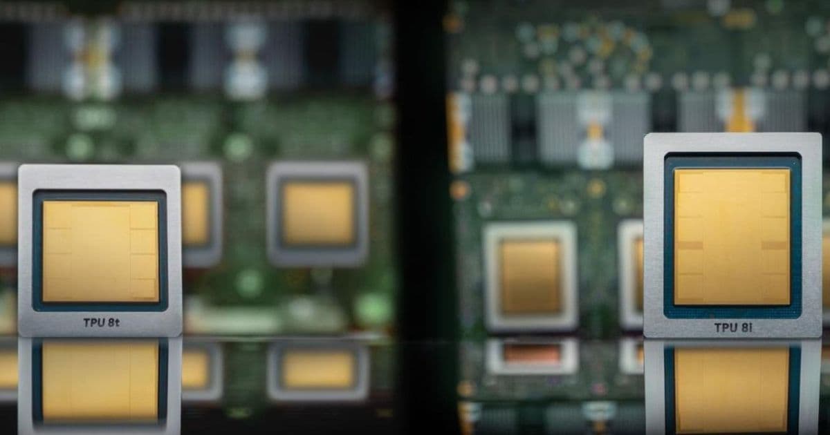
Google has transitioned its AI hardware strategy from a unified chip design to a bifurcated approach with the introduction of the TPU 8t and TPU 8i. This shift marks the first time in the decade-long history of the Tensor Processing Unit program that Google is shipping two distinct silicon designs to address the diverging requirements of large-scale model training and low-latency inference.
Technical Specifications and Performance Trade-offs
Both the TPU 8t and 8i are fabricated using TSMC's N3 process family and utilize HBM3E memory. However, the raw compute figures reveal a strategic decision to prioritize cost and yield over peak per-socket performance.
- TPU 8t (Training): Delivers 12.6 FP4 PFLOPs with 216 GB of HBM3e running at 6,528 GB/s. It retains the 3D Torus interconnect and SparseCore for irregular memory access patterns during embedding lookups.
- TPU 8i (Inference): Delivers 10.1 FP4 PFLOPs with 288 GB of HBM3e at 8,601 GB/s and 384 MB of on-chip SRAM.
When compared to competitors, the gap in raw compute is significant. Nvidia's Vera Rubin R200 is rated at 35 FP4 PFLOPs, and AMD's MI455X reaches 40 FP4 PFLOPs. This represents a roughly 3:1 performance gap per socket. Google's choice of HBM3E over HBM4 is a calculated trade-off. For the TPU 8t, memory bandwidth is actually 11.5% lower than the previous Ironwood generation, a move intended to increase wafer yields and reduce the cost per chip.
Architectural Shift: Boardfly vs. 3D Torus

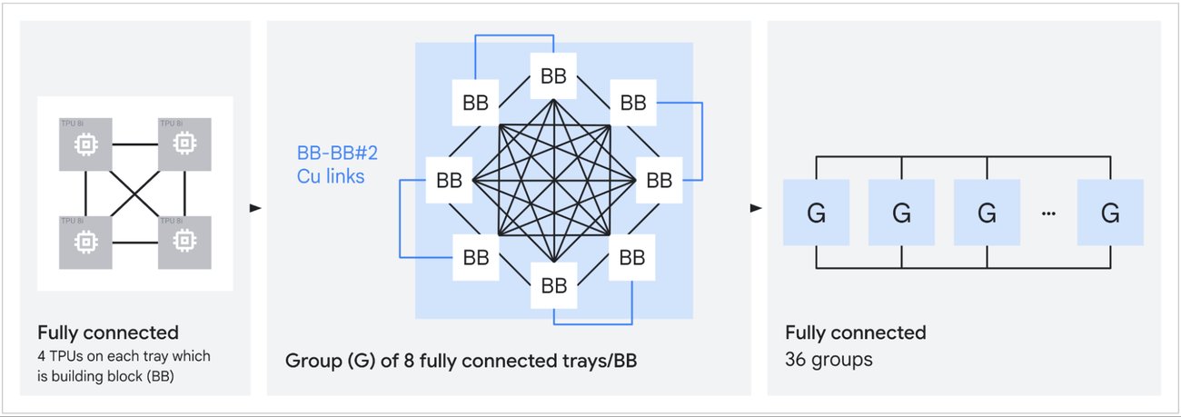
The most significant technical departure is found in the TPU 8i. While previous generations relied on a 3D Torus interconnect, the 8i introduces "Boardfly," a topology inspired by the Dragonfly architecture.
Boardfly utilizes a three-tier hierarchy: four-chip building blocks connected into 32-chip groups via copper cabling, which are then linked by optical circuit switches into pods of up to 1,024 chips. This reduces the worst-case packet path from 16 hops in a 3D Torus to just seven. This 56% reduction in network diameter is critical for Mixture-of-Experts (MoE) models, where token routing requires frequent all-to-all communication across unpredictable chip pairs.
Furthermore, the TPU 8i replaces SparseCore with a Collectives Acceleration Engine (CAE). The CAE offloads reduction and synchronization operations during autoregressive decoding, reducing on-chip collective latency by up to five times. Combined with tripled SRAM for larger KV cache storage, Google claims an 80% improvement in performance per dollar for MoE models compared to Ironwood.
Scaling and Supply Chain Dynamics
Google's primary competitive advantage is not the individual chip, but the scale of the cluster. A TPU 8t superpod integrates 9,600 chips with two petabytes of shared HBM. The new Virgo Network fabric allows for the interconnection of up to 134,000 TPU 8t chips in a non-blocking data center fabric, with the ability to scale beyond 1 million chips across multiple sites. This contrasts sharply with current Nvidia NVLink deployments, which typically top out at 576 accelerators.
To support this scale, Google has diversified its silicon design partnerships. While Broadcom has been the exclusive partner since 2015 and continues to handle the TPU 8t, MediaTek has joined to design the TPU 8i. This dual-sourcing strategy is estimated to reduce per-chip costs by up to 30%.
Market Implications
This hardware evolution aligns with Google's broader cloud strategy. By offering both TPU 8 and Nvidia Vera Rubin instances over the same Virgo Network fabric, Google is positioning itself as a flexible provider rather than trying to replace Nvidia entirely.
The commercial demand is already evident through massive capacity commitments. Anthropic has a 3.5 GW TPU capacity commitment starting in 2027, while Meta is expected to rent between 500,000 and 800,000 TPU chips by 2027. Additionally, Apple is utilizing TPU infrastructure for Gemini-powered Siri workloads, a deal valued at approximately $1 billion annually.
By shifting the battleground from per-chip TFLOPS to cluster-wide throughput and cost-efficiency, Google is optimizing for the actual economics of LLM deployment at a planetary scale.
Comments
Please log in or register to join the discussion