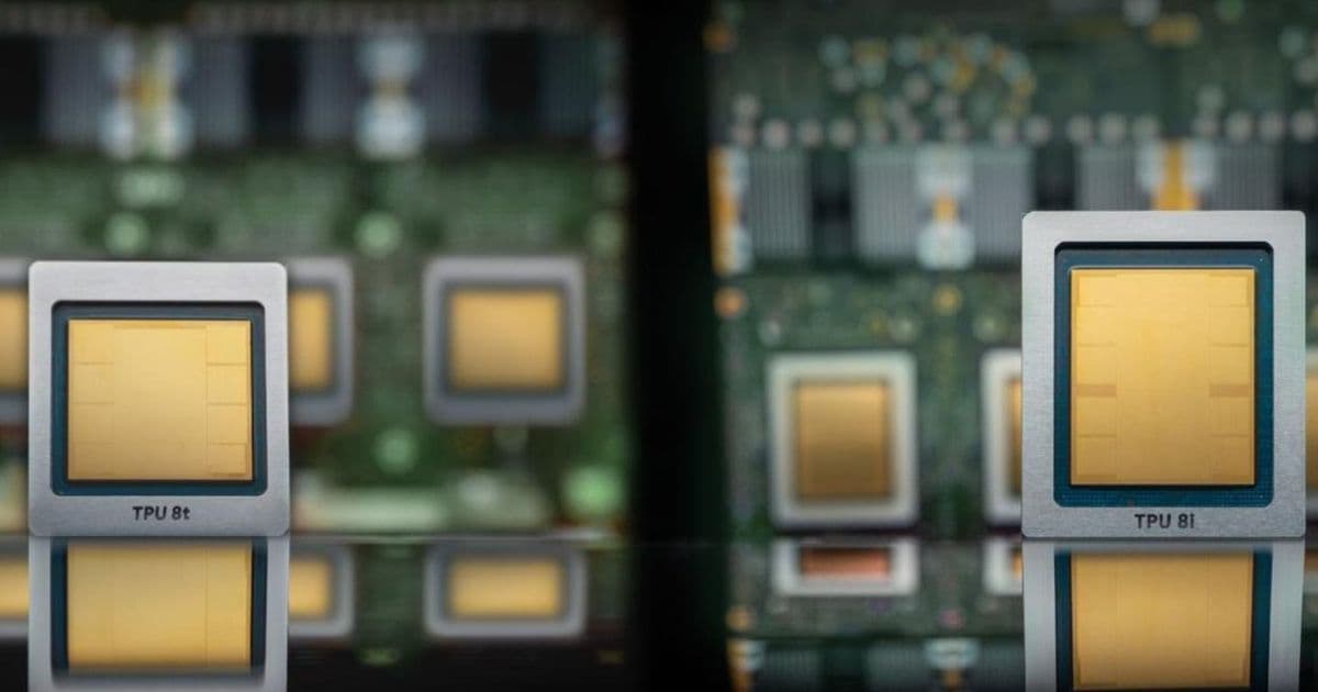
Google has reportedly committed Intel to packaging over 3 million TPUs in 2028, while SK hynix qualifies whether high-bandwidth memory holds up on Intel's EMIB. The orders signal the first serious crack in TSMC's CoWoS monopoly, where Nvidia alone absorbs roughly 60% of global capacity.
Google has placed an order for Intel to package more than 3 million of its Tensor Processing Units in 2028, following months of testing Intel's advanced packaging technology, according to a report from The Information citing four people familiar with the matter. The same sources indicate that Nvidia is evaluating Intel to build a future processor fusing four GPU dies into a single unit, tied to its Feynman architecture due in 2028, and that SK hynix is testing whether its high-bandwidth memory operates reliably on Intel's packaging.
The figures matter because they convert what were described in April as "active discussions" between Intel and hyperscalers like Google and Amazon into a concrete unit count and a production timeline. The added wrinkle is the SK hynix qualification, which would ultimately determine whether any of this packaging reaches Nvidia accelerators at all.
The context here is a supply bottleneck that has defined AI hardware procurement for two years. TSMC's Chip-on-Wafer-on-Substrate process, CoWoS, is the industry standard for stitching logic dies and memory stacks into a single accelerator package, and it has been oversubscribed since 2023. Intel's embedded multi-die interconnect bridge, or EMIB, is the only alternative that AI chip makers can realistically qualify at volume before the end of the decade.
A queue concentrated in a few hands
CoWoS demand is dominated by a handful of buyers. Nvidia is expected to account for roughly 60% of global CoWoS consumption this year, with Broadcom and AMD splitting another 26% between them. That leaves custom-ASIC designers and smaller AI chip makers waiting behind the largest GPU order book in the industry.
The hyperscalers building their own silicon cannot afford to wait. Companies with multimillion-unit roadmaps need a second packaging source rather than capacity TSMC has signaled will stay tight for years. That structural shortage is what makes Intel's foundry pitch viable despite its financial troubles, which I will get to below.
How EMIB differs from CoWoS
The two approaches solve the same problem in opposite ways. CoWoS mounts every die on a large silicon interposer, and all signals and power must traverse that interposer. Because the interposer scales with package size, reticle-class designs waste silicon at the edges. EMIB embeds small silicon bridges directly in the organic substrate, placed only where two dies need to connect, with no interposer underneath at all.
Intel cites package utilization near 90% for EMIB against roughly 60% for interposer-class packaging, since small bridges tile efficiently while large interposers do not. Bernstein analysts estimate EMIB costs a few hundred dollars per chip versus $900 to $1,000 for CoWoS on a Rubin-class processor, though the firm cautions that the estimate suffers from a lack of external production track record.
The trade-off sits in power delivery. Standard EMIB routes power around the bridge through the substrate along long, resistive paths. That was acceptable for older parts like Sapphire Rapids and Ponte Vecchio, but not for HBM4-class accelerators that draw far more current. EMIB-T addresses this by adding through-silicon vias to the bridge die for vertical power delivery, and it is set to enter fab rollout this year. Intel says EMIB-T supports HBM3, HBM3E, HBM4, and future HBM5 stacks, and scales to a 120mm x 180mm package carrying more than 38 bridges and over 12 reticle-sized dies. Jaguar Shores, the successor to the canceled Falcon Shores accelerator, is the likely first product to use it.
The SK hynix gate
SK hynix sits at the center of whether Intel's packaging reaches flagship silicon. The company held a 57% share of HBM revenue in Q4 2025 per Counterpoint Research, and UBS expects it to take roughly 70% of the HBM4 supplied for Nvidia's Rubin platform this year. When SK hynix decides whether its memory works reliably on EMIB, it is effectively deciding for a large slice of the market.
HBM is itself a packaging problem. Each stack is multiple memory dies bonded vertically through TSVs, then mounted next to a host processor with tight tolerances on power and thermal behavior. Validating those stacks on EMIB rather than a CoWoS interposer is the real test of whether Intel can package memory to the standard Nvidia and Google demand. An official sign-off from SK hynix, or a working HBM4-on-EMIB-T production result, would move Intel's packaging from "tested" to "trusted."
Until that happens, the split between accelerator types holds. ASIC designers running lower memory bandwidth, including Google and Meta, can adopt EMIB sooner, while bandwidth-bound GPUs stay on CoWoS longer.
Intel still has to prove it
No named external AI customer is in EMIB or Foveros volume production today. Intel runs EMIB in its own server CPUs, including the 18A Clearwater Forest part whose 17-tile package uses 12 bridges, but every named outside engagement so far, including Google's order, points to 2027 or 2028 products or remains an evaluation.
The financial picture underscores the stakes. Intel Foundry lost $10.3 billion on $17.8 billion of revenue in 2025. In Q1 2026, the division posted $5.4 billion in revenue against a $2.4 billion operating loss, with external customers accounting for just $174 million of that total. CFO David Zinsner told the Morgan Stanley TMT conference in March that the foundry is close to closing deals worth "billions per year in terms of revenue" on advanced packaging alone, up from a pipeline he had earlier measured in the hundreds of millions.
Yields are the other open question. Intel uses 18A, its first node with gate-all-around transistors and backside power delivery, for Panther Lake and Clearwater Forest, treating its own products as a proving ground before courting external logic customers. The company's most recent guidance puts yield improvement at 7 to 8 percent per month, accelerated by closer cooperation with external partners.
For buyers, the calculus is straightforward. A second packaging source that costs a fraction of CoWoS and sidesteps a multi-year queue is worth qualifying even with execution risk attached. The 3 million TPU figure, if it holds, is the clearest sign yet that the largest AI customers are willing to bet on it.
Comments
Please log in or register to join the discussion