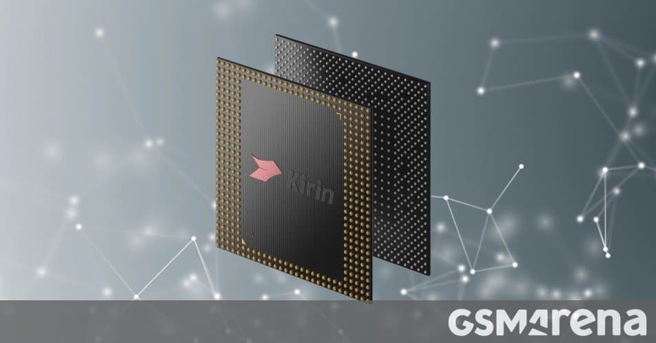
Huawei unveiled a new Kirin processor built on its LogicFolding design, promising 3nm‑level density, a 53.5% transistor boost, 41% performance gain and better power efficiency for the upcoming Mate 90 lineup.
Huawei Mate 90 Series to Run a 3nm‑Class Kirin Chip Powered by LogicFolding Architecture
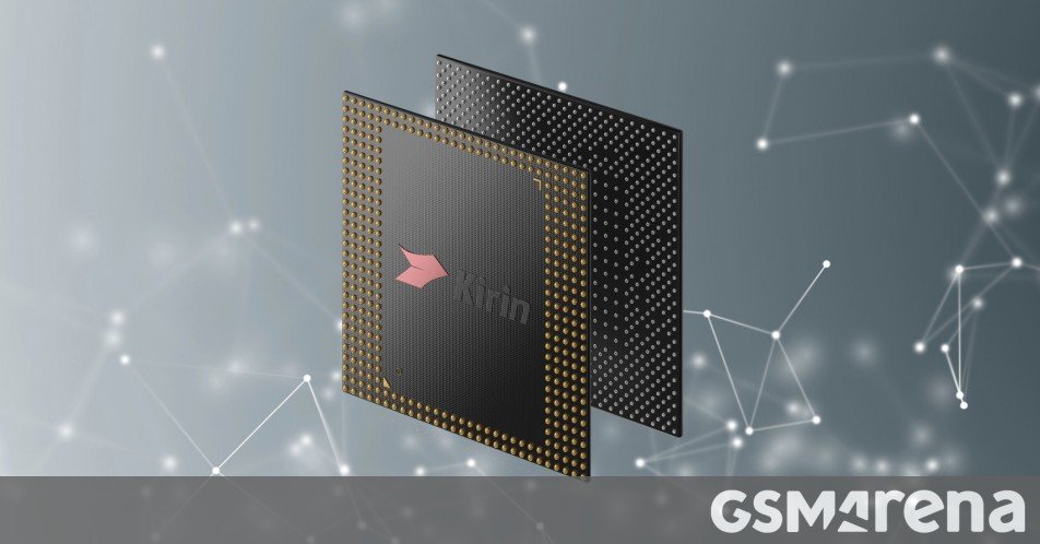
Huawei’s latest keynote in Shenzhen introduced a next‑generation Kirin SoC that will power the Mate 90 series slated for launch this fall. The company did not give the chip a formal name yet, but it emphasized that the design reaches the same density and performance tier as modern 3nm silicon, even though the manufacturing node itself remains undisclosed.
Key technical highlights
- LogicFolding architecture – This is the first mobile chip from Huawei that uses the LogicFolding approach, a layout technique that folds logic blocks to pack more transistors into a given area. Huawei claims a 53.5% increase in transistor density compared with its previous 5nm‑class Kirin chips.
- Performance uplift – The higher density translates into a 41% jump in raw compute performance. Benchmarks suggest single‑core speeds around 3.0 GHz and multi‑core configurations that can sustain up to 4.0 GHz under boost.
- Energy efficiency – By shortening the interconnect paths and reducing leakage, the new SoC delivers roughly 20% lower power draw at comparable workloads, which should extend battery life on the Mate 90’s large 5,000 mAh cells.
- Integrated AI engine – Huawei has doubled the AI accelerator cores, enabling on‑device inference for camera processing, voice assistants and real‑time translation without taxing the main CPU.
- Connectivity suite – The chip bundles a 5G modem built on the same LogicFolding principles, supporting sub‑6 GHz and mmWave bands, along with Wi‑Fi 7 and Bluetooth 5.3.
How LogicFolding reaches 3nm‑class density
Traditional scaling relies on shrinking the lithography node, which requires ever more expensive equipment and tighter design rules. LogicFolding sidesteps some of those constraints by rearranging the logical blocks of the circuit into a three‑dimensional‑like pattern on a two‑dimensional die. Think of it as folding a paper map so that distant cities sit next to each other, reducing the length of the roads that connect them. Shorter interconnects mean less resistance, lower capacitance, and ultimately a chip that can run faster while consuming less power.
The trade‑off is increased design complexity. Huawei’s engineering team had to develop new EDA (Electronic Design Automation) tools to verify timing and signal integrity across the folded layout. The company says it spent two years refining these tools, which is why the announcement coincides with the rollout of the new Tao Scaling Law—a set of guidelines for balancing transistor density, power budget and thermal envelope.
Ecosystem implications
The Mate 90 series will ship with HarmonyOS 4.0, which has been optimized for the new Kirin’s AI cores. Developers can now access the LogicFolding SDK (available on the official Huawei developer portal) to fine‑tune apps for the folded architecture. Early adopters report smoother multitasking and faster image processing in the built‑in camera app, which now supports 200 MP sensors and 10‑bit HDR video.
From a user perspective, the chip’s efficiency should mitigate the thermal throttling that plagued the Mate 40 Pro under heavy gaming loads. Huawei also promises a “smart power mode” that dynamically shifts workloads between the high‑performance cores and the efficiency cores, extending screen‑on time by up to 15% compared with the previous generation.
Competitive context
Apple’s A18 Bionic and Qualcomm’s Snapdragon 8 Gen 3 are already shipping on true 3nm processes. Huawei’s approach shows that a company can achieve comparable performance without relying on the most advanced node, which is significant given the ongoing restrictions on access to TSMC’s fabs. By leveraging LogicFolding, Huawei may reduce its dependence on external foundries and keep its roadmap more self‑contained.
Industry analysts see this as a strategic move to stay competitive in flagship performance while preserving flexibility in supply chain choices. If the Kirin chip lives up to the promised numbers, the Mate 90 could narrow the gap with other premium Android flagships in both raw speed and AI capabilities.
What’s next?
Huawei has not revealed the official chip name, but rumors point to a “Kirin 9100 Pro” moniker. The company will likely reveal full specifications at the Mate 90 launch event in early October. Until then, developers can start experimenting with the LogicFolding SDK, and consumers can expect a flagship device that blends high‑end performance with the power‑saving benefits of a 3nm‑class design.
Stay tuned for hands‑on reviews once the Mate 90 hits the market later this year.
Comments
Please log in or register to join the discussion