
Intel says its 18A-P process gives chip designers more speed at the same power and keeps 18A design rules, a key test for its foundry push.
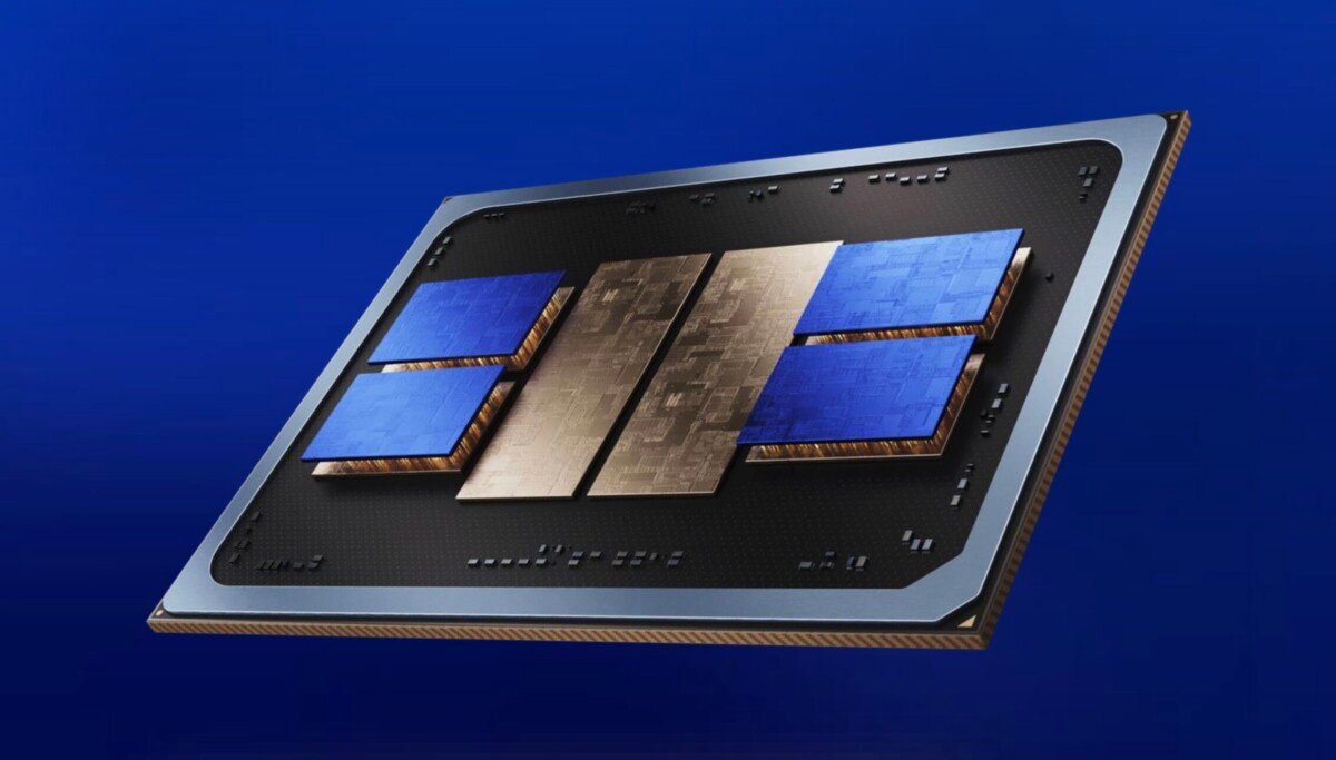
Intel has begun risk production of 18A-P, an enhanced version of its 18A chipmaking process, as the company tries to convince outside customers that its foundry business can deliver advanced silicon on schedule.
Intel disclosed the milestone Wednesday, June 17, 2026, at the IEEE 2026 VLSI Symposium in Hawaii. Risk production gives Intel and its customers low-volume chips that engineers can qualify before volume manufacturing.
Intel says 18A-P can deliver 9% higher performance at the same power as 18A, or 18% lower power at the same performance. The company credits transistor, interconnect and design technology changes for the gains.
The design-rule compatibility may matter more to foundry customers than the headline speed figure. Intel says customers that design chips for 18A can move those designs to 18A-P with limited changes. That gives chip designers a path to better performance without restarting large parts of the design process.
Intel needs that promise to hold. The company has spent years trying to turn Intel Foundry into a credible rival to Taiwan Semiconductor Manufacturing Co. and Samsung. Outside customers need process maturity, stable tools and predictable schedules before they commit expensive chip programs.
Intel launched its first 18A chips in January with Panther Lake Core Ultra Series 3 processors. The company now wants 18A-P to help attract external foundry work. Industry reports have linked Intel to possible Apple manufacturing discussions, though neither company has announced a customer deal for 18A-P.
Intel also plans an 18A-PT variant for designs that use through-silicon vias. That technology helps engineers stack chiplets and memory tiles in advanced packages, a design pattern that AI accelerator makers use to move data between compute and memory with less delay.
Intel executives have acknowledged that 18A strained the company. Chief Financial Officer David Zinsner said earlier this month that Intel tried to improve performance and yield at the same time, which slowed the program.
Intel used the VLSI event to show work beyond 18A-P, including complementary FET technology with stacked NMOS and PMOS devices, plus gallium nitride power devices integrated with silicon logic. Those projects point to future density and power gains, but Intel’s foundry credibility now rests on customers seeing working 18A-P silicon and predictable yields.
For chip buyers, the compliance question comes first. A faster process helps if engineers can move a design without adding months of verification work. Intel says 18A-P gives customers that option. Customers will now test that claim in silicon.
Comments
Please log in or register to join the discussion