Intel needs 14A customers, 18A yield gains and tax-credit timing to line up before it commits the next wave of leading-edge fab capacity.

Intel faces a capacity puzzle that its own customers will help solve. The company has cut European projects, bought back control of Ireland’s Fab 34 and kept Ohio on a slow buildout while it waits for 14A customers to commit volume.
The next six months matter because two clocks now point at the same set of fabs. Intel Chief Executive Lip-Bu Tan has told investors that prospective 14A customers will make supplier decisions from the second half of 2026 into the first half of 2027. Congress set a separate Dec. 31, 2026 construction-start cutoff for the 35% advanced manufacturing investment credit under Section 48D. Intel can preserve public support for new U.S. fab shells if it starts qualifying work before that date.
Intel’s near-term manufacturing base now rests on Arizona, Oregon, Ohio, New Mexico and Ireland. Chandler, Arizona carries the main 18A ramp. Hillsboro, Oregon develops 14A and houses Intel’s High-NA EUV work. New Albany, Ohio gives Intel room for 14A and later nodes if customers commit. Leixlip, Ireland gives Intel EUV-class European capacity on Intel 4 and Intel 3. Rio Rancho, New Mexico handles high-volume Foveros packaging in the United States.
| Site | Fab | Node focus | Status |
|---|---|---|---|
| Chandler, Arizona | Fab 52 | Intel 18A | Intel uses it for 18A ramp and Panther Lake compute tiles |
| Chandler, Arizona | Fab 62 | Unassigned, 18A-capable | Intel targets readiness around 2028 |
| Hillsboro, Oregon | D1X | 18A volume support, 14A development | Intel develops 14A there with High-NA EUV tools |
| New Albany, Ohio | Mod 1 | 14A and later nodes | Intel targets completion in 2030 and operations in 2030-31 |
| New Albany, Ohio | Mod 2 | 14A and later nodes | Intel targets completion in 2031 and operations in 2032 |
| Leixlip, Ireland | Fab 34 | Intel 4, Intel 3 | Intel regained full ownership in April 2026 |
| Rio Rancho, New Mexico | Fab 9 | Foveros packaging | Intel runs high-volume advanced packaging there |
Arizona carries the 18A ramp
Intel built Fab 52 at its Ocotillo campus in Chandler as the production base for its first high-volume 18A products. The fab supports Panther Lake compute tiles and Clearwater Forest server parts, which put Intel’s RibbonFET gate-all-around transistors and PowerVia backside power delivery into commercial silicon.
Intel has described Fab 52 as capable of more than 10,000 18A wafer starts per week at full ramp. That figure equals about 40,000 wafer starts per month, which would make the site one of the largest advanced-node fabs in the United States. Output still depends on yield, product mix and tool availability, so named capacity does not equal shipped CPU volume.
Tan has said Intel improves 18A yields by 7% to 8% per month. Intel needs those gains because a young node can leave expensive EUV capacity idle while engineers tune defect density, parametric variation and process control. A fab can own enough tools on paper and still ship fewer good dies if engineers lose too many chips per wafer.
Intel has also moved 18A-P into risk production, according to recent public reporting. That variant targets higher performance and lower power than baseline 18A while keeping design compatibility. For foundry customers, compatibility matters because a drop-in node variant lets design teams reuse more IP, verification work and physical design effort.
Fab 62 gives Intel an option around 2028. Intel has not assigned the fab to a public node. The company can use it as extra 18A capacity if external demand appears, or it can hold the shell for 14A if Ohio cannot support an earlier ramp. Brookfield Infrastructure helped finance the Arizona expansion through a joint venture, so Intel must share economics from those fabs under that agreement.
Oregon owns the 14A learning curve
Intel develops leading-edge processes at the D1X complex in Hillsboro. That gives Oregon the first 14A burden: Intel’s engineers must prove the node before Intel moves the recipe into a high-volume fab.
14A matters because Intel designed it around High-NA EUV. ASML’s High-NA tools use a larger numerical aperture than current EUV scanners, which can print smaller features with less multi-patterning on selected layers. That can reduce process complexity, but it also raises tool cost and introduces new mask, resist and overlay challenges. ASML explains the technology in its High-NA EUV overview.
Intel has tied 14A to second-generation RibbonFET devices, PowerDirect backside power delivery and performance-focused cell libraries. The company’s Intel Foundry process roadmap places 14A after the 18A family. Intel needs external customers because the R&D cost, High-NA tool cost and fab shell cost exceed what its own CPU roadmap can support with comfort.
A process design kit sits at the center of that customer decision. A PDK gives chip designers the models, design rules, standard cells, SRAM compilers and verification decks they need to build a product for a foundry process. Customers cannot commit high-volume chips on slogans. They need timing models, power estimates, layout rules and signoff flows that match silicon.
Tan has pointed to the 14A v0.9 PDK as the key customer milestone, with external delivery targeted for October. Cadence said June 8 that it had reached a multiyear agreement with Intel Foundry to support 14A design technology co-optimization and production-ready PDK work. That EDA support gives fabless customers a path from test chips to product tape-outs, assuming Intel’s silicon data supports the models.
Ohio gives Intel scale if customers sign
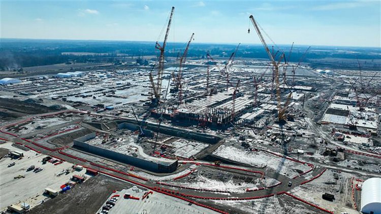
Intel’s Ohio One campus in New Albany gives the company its largest U.S. expansion option. Intel broke ground in 2022 on a first phase worth more than $28 billion, with two fabs and room across the site for up to eight fabs. Intel first talked about production in the middle of the decade. In February 2025, Chief Global Operations Officer Naga Chandrasekaran moved the schedule out: Mod 1 completion in 2030, operations in 2030-31, Mod 2 completion in 2031 and operations in 2032.
That delay tells customers and investors the same thing. Intel will not fill Ohio with leading-edge tools until it sees demand that can carry depreciation. A modern logic fab can cost tens of billions of dollars before a customer sees the first qualified wafer. Empty shells burn cash. Fully equipped fabs burn far more if customers do not load them.
Intel has spent about $5 billion in Ohio, including about $1.4 billion in 2025. Bechtel has continued construction hiring, and Intel still presents Ohio as a 14A and future-node site. The company can accelerate work if a customer signs a volume deal, but it needs that commitment soon enough to order tools, build cleanroom infrastructure and meet tax-credit timing.
The first named 14A interest has come from Elon Musk’s planned TeraFab project for AI chips. That creates a public reference point, but Intel’s filings point to the need for a significant external customer. A future test-production plan does not carry the same weight as a near-term wafer volume commitment with deposits, design milestones and yield-linked purchase terms.
Ohio also gives Intel geographic leverage. U.S. policymakers want more advanced-node manufacturing inside the country, and Intel’s Ohio project page frames the site as a long-term domestic manufacturing hub. Intel still has to match that policy value with customers who will pay for wafers.
Ireland shifts back under Intel control
Intel’s Fab 34 in Leixlip remains its central EUV-class manufacturing site in Europe. The fab produces Intel 4 and Intel 3 silicon for Core Ultra and Xeon 6 products. Intel opened the expansion in 2023 after years of construction and tool installation at its Ireland campus.
In 2024, Apollo-managed funds paid $11.2 billion for a 49% stake in a joint venture tied to Fab 34 output. Intel used that structure to raise cash while keeping operational control. In April 2026, Intel agreed to buy the stake back for $14.2 billion, funded with cash and about $6.5 billion in new debt.
That price gave Apollo a gain of about 27% in less than two years. Intel paid the premium because Fab 34’s wafer economics matter more after the company cut other European capacity plans. Intel canceled Magdeburg, Germany and Wroclaw, Poland in July 2025 after it failed to secure enough committed demand. Magdeburg would have supported 14A-era production with about 10 billion euros in German subsidies attached. Wroclaw would have added assembly and test capacity near the German fab.
Those cancellations left Intel with one leading-edge European fab. Fab 34 cannot solve 14A capacity by itself because it runs Intel 4 and Intel 3, but full ownership gives Intel more control over margin, wafer allocation and strategic planning in Europe.
Packaging decides product capacity too
Intel’s front-end fab map tells only part of the supply story. Tiled products need advanced packaging capacity, and Intel’s client and server roadmaps depend on Foveros and EMIB.
Fab 9 in Rio Rancho handles high-volume Foveros 3D stacking in the United States. Intel uses Foveros to bond compute, graphics and I/O tiles into one package. Meteor Lake proved that model in client PCs. Clearwater Forest extends the approach into high-core-count server silicon, where Intel stacks and connects tiles to raise density without forcing one giant die onto a single process.
Rio Rancho matters because Intel has cut or delayed other packaging options. The company consolidated Costa Rica assembly and test work into Vietnam and Malaysia. Intel paused the $7 billion Penang expansion in Malaysia in early 2025, then revived it with first-phase assembly and test operations due later in 2026. Intel has also outsourced EMIB production to Amkor’s Songdo facility in South Korea.
Packaging creates its own bottlenecks. A fab can produce good compute tiles, and Intel can still miss product demand if substrates, interposers, hybrid bonding tools or test capacity lag. AI servers have made that constraint more visible across the industry because customers buy finished systems, not loose wafers.
Tax credits put a date on fab choices
The Section 48D advanced manufacturing investment credit gives Intel a strong reason to start qualifying construction before Dec. 31, 2026. Congress raised the credit from 25% to 35%, but the law still cuts off property whose construction begins after that date. The CHIPS for America program and related tax support have become part of Intel’s fab economics.
Treasury rules allow companies to qualify through physical work or a 5% safe harbor. That means Intel can preserve the credit for a new shell if it spends enough or starts enough qualifying work before the deadline. The rule does not force Intel to equip the fab at once, but it gives the company a reason to move early on shells in Arizona, Oregon or Ohio.
The U.S. government also holds an equity stake in Intel after converting unpaid CHIPS grants and Secure Enclave funds into shares. That makes Intel’s construction choices a matter for shareholders, customers and policymakers at the same time. Intel needs the credit to improve fab economics, and Washington needs Intel to turn public support into domestic wafer output.
Three signals will show Intel’s direction
A named 14A customer with committed volume would give Intel the clearest signal. Test chips and evaluation programs matter, but Intel needs purchase commitments that justify tools, staffing and construction acceleration. Without that customer, Intel has warned that it may pause or discontinue 14A, successor nodes and related manufacturing expansion projects.
A construction-start announcement before Dec. 31 would show which site Intel wants to protect under the 35% credit. Ohio offers the largest long-term upside. Arizona offers a nearer path because Intel already has an 18A ecosystem there. Oregon gives Intel process-development strength but not the same high-volume role.
18A yield progress will shape the whole decision. If Intel raises yields on schedule, Fab 52 can support more Panther Lake and Clearwater Forest output, and Fab 62 can wait for the right assignment. If yield learning drags, Intel may need more near-term 18A capacity before it can shift attention to 14A.
Intel has spent years telling customers that it can return to process leadership. The next phase asks customers to decide with wafers, masks and money. Intel can build the shells, buy the tools and publish the roadmaps. Customers will decide whether 14A gets a full production network.
Comments
Please log in or register to join the discussion