German nanofabrication consortium LAB14 joins MIT.nano, contributing cutting-edge maskless stepper and XPS/HAXPES tools to advance micro- and nanotechnology research at MIT.
The advanced manufacturing group becomes a member and will contribute equipment to MIT.nano.

Amanda Stoll DiCristofaro | MIT.nano
Publication Date : March 3, 2026
PRESS INQUIRIES
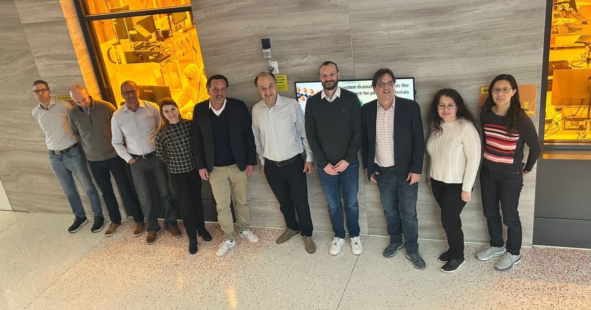
Caption : LAB14 GmbH, a corporate network based in Germany that unites eight high-tech companies focused on nanofabrication, microfabrication, and surface analysis, has joined the MIT.nano Consortium. Seen here in front of MIT.nano’s cleanroom are (from left to right): Jorg Scholvin of Fab.Nano, Gregg Moore of Heidelberg Instruments, Christian Bach of Heidelberg Instruments USA, Jenny Rittmaier of LAB14, Martin Wynaendts van Resandt of LAB14, Vladimir Bulović of MIT.nano, Steffen Diez of LAB 14, Niels Wijnaendts van Resandt of LAB14, Anna Osherov of Characterization.nano, and Joyce Wu of MIT.nano. Credits : Photo courtesy of MIT.nano.
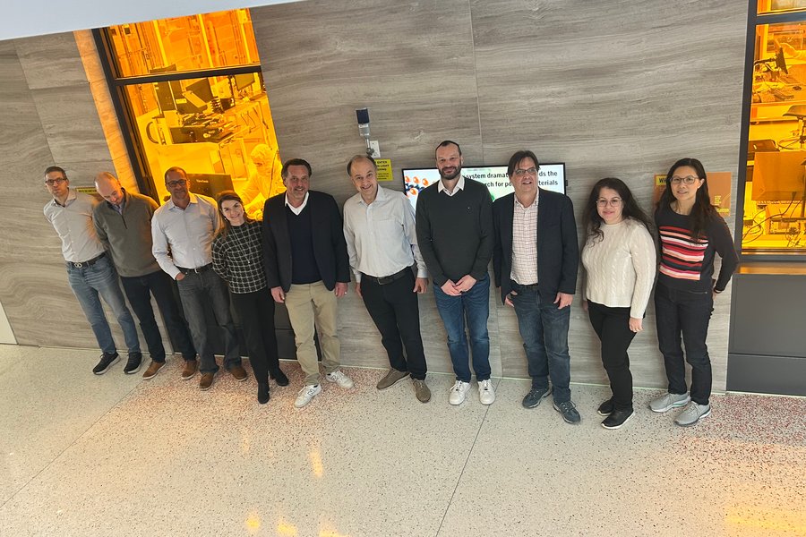
Caption : Jorg Scholvin, associate director for Fab.nano, shows LAB14 representatives where the new VPG 300 DI maskless stepper will be positioned inside MIT.nano’s cleanroom. Credits : Photo courtesy of MIT.nano.
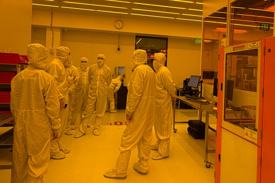
Caption : Members of LAB14 pose on one of MIT.nano’s fan decks. This space is essential for maintaining the pristine environment in the cleanroom. Here, equipment cleans and replaces the air in the research space below every 15 seconds. Credits : Photo courtesy of MIT.nano.
LAB14 GmbH, a corporate network based in Germany that unites eight high-tech companies focused on nanofabrication, microfabrication, and surface analysis, has joined the MIT.nano Consortium.
"The addition of LAB14 to the MIT.nano Consortium reinforces the importance of collaboration to advance the next set of great ideas," says Vladimir Bulović, the founding faculty director of MIT.nano and the Fariborz Maseeh (1990) Professor of Emerging Technologies at MIT. "At MIT.nano, we are thrilled when our shared-access facility leads to cross-disciplinary discoveries. LAB14 carries this same motivation by assembling the constellation of remarkable interconnected industry partners."
Comprising eight companies — Heidelberg Instruments, Nanoscribe, GenISys, Notion Systems, 40-30, Amcoss, SPECSGROUP, and Nanosurf — LAB14 is focused on developing products and services that are fundamental to micro- and nanofabrication technologies, supporting industrial and research-driven applications with complex manufacturing and analysis requirements. The companies of LAB14 operate under a shared organizational structure that enables closer coordination in technology development. This setup allows for faster research progress and more efficient manufacturing workflows.
"Joining the MIT.nano Consortium marks a significant milestone for LAB14 and our companies," says Martin Wynaendts van Resandt, CEO of LAB14. "This participation allows our network to collaborate directly with world-leading researchers, accelerating innovation in micro- and nanotechnology."
As part of this engagement, LAB14 will provide two pieces of equipment to be installed at MIT.nano within the coming year.
Advanced Tools for Cutting-Edge Research
The VPG 300 DI maskless stepper, a high-performance, direct-write system from Heidelberg Instruments, will be positioned inside MIT.nano’s cleanroom. This tool will allow MIT.nano users to pattern structures smaller than 500 nanometers directly onto wafers with accuracy and uniformity comparable to typical high resolution i-line lithography. Equipped with advanced multi-layer alignment and mix‑and‑match functions, the VPG creates a seamless link between laser direct writing and e‑beam lithography.
The EnviroMETROS X-ray photoelectron spectroscopy (XPS/HAXPES) tool by SPECSGROUP will join the suite of Characterization.nano instruments. This unique system is specialized in nondestructive depth profile measurements using multiple X-ray energies to determine the thickness of thin-film samples and their chemical compositions with highest precision. It supports various analyses across a wide pressure range, allowing MIT.nano users to examine thin‑film materials under more realistic environmental conditions and to observe how they change during operation.
The MIT.nano Consortium: A Platform for Innovation
The MIT.nano Consortium is a platform for academia-industry collaboration, fostering research and innovation in nanoscale science and engineering. Consortium members gain unparalleled access to MIT.nano and its dynamic user community, providing opportunities to share expertise and guide advances in nanoscale technology.
MIT.nano continues to welcome new companies as sustaining members. For details, and to see a list of current members, visit the MIT.nano Consortium page.
SHARE THIS NEWS ARTICLE ON:
X Facebook LinkedIn Reddit Print
RELATED LINKS
RELATED TOPICS
MIT.nano Nanoscience and nanotechnology Industry Fabrication Collaboration
RELATED ARTICLES
SLB joins the MIT.nano Consortium MIT, Applied Materials, and the Northeast Microelectronics Coalition Hub to bring 200mm advanced research capabilities to MIT.nano Shell joins MIT.nano Consortium
Comments
Please log in or register to join the discussion