MIT.nano has installed a state-of-the-art molecular beam epitaxy (MBE) system that will enable researchers to study quantum materials at the atomic level, addressing critical challenges in quantum computing development.
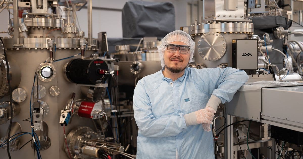
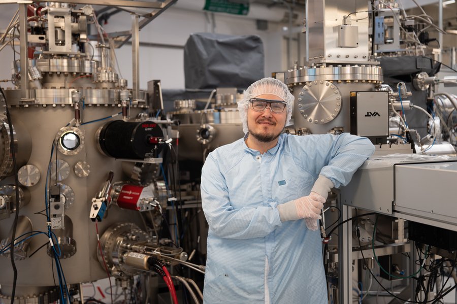
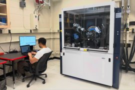
A complex piece of equipment recently installed in MIT.nano's first-floor cleanroom represents a significant advancement in quantum materials research. The new molecular beam epitaxy (MBE) system, a custom-built physical vapor deposition apparatus operating under ultra-high vacuum conditions, will allow scientists to grow and analyze high-quality thin films essential for developing more robust quantum bits (qubits).
"To realize the full promise of quantum computing, we need to build qubits that are robust, reproducible, and extensible," explains William D. Oliver, the Henry Ellis Warren (1894) Professor of Electrical Engineering and Computer Science and professor of physics at MIT. "To date, most of the improvements to superconducting qubit performance are traceable to circuit design—essentially, designing qubit circuits that are less sensitive to their environmental noise. However, those improvements have largely run their course. Going forward, we need to address the fundamental materials science and fabrication engineering required to reduce the sources of environmental noise."
The MBE Quantum system, manufactured by DCA, represents exactly the right tool at this critical juncture in quantum computing development. As the largest single deposition chamber (1-meter diameter) the company has sold in the United States, it brings unprecedented capabilities to MIT researchers.
Technical Capabilities: A Multi-Chamber Approach
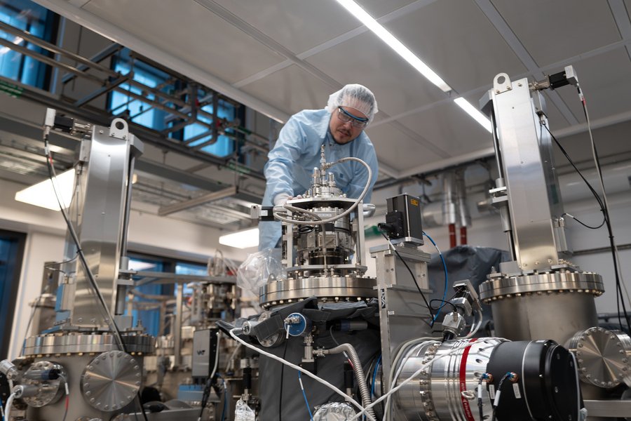
The system, occupying 600 square feet, consists of six interconnected chambers that work in concert to enable precise materials growth and analysis:
Load Lock: Where wafers are introduced and brought down from atmospheric pressure to near-space-level vacuum conditions.
Distribution Center: Acts as a central hub, transferring wafers between chambers while maintaining the ultra-high vacuum environment.
Deposition/Growth Chamber: The primary chamber where atoms of superconducting metals are precisely deposited onto substrates, typically silicon, at the atomic scale.
Oxidation Chamber: Facilitates the growth of key ceramic materials essential for qubit functionality.
Storage Chamber: Can hold an additional 10 wafers within the vacuum environment for later processing.
X-ray Photoelectron Spectroscopy (XPS) Chamber: A unique feature allowing researchers to analyze the material structure without breaking the vacuum environment.
"Think of this system like an inverted International Space Station (ISS)," describes Patrick Strohbeen, research scientist in the EQuS group. "The ISS is a small chamber of atmosphere surrounded by the vacuum of space. This MBE system is a chamber of space-level vacuum surrounded by atmosphere."
The system maintains a steady negative 90 degrees Celsius within its vacuum chamber, enabling the precise growth of crystalline materials. This extreme environment is crucial for studying quantum materials, where even minor impurities or defects can significantly impact quantum properties.
Real-World Applicability: Addressing Quantum Computing Challenges
Quantum bits, or qubits, are incredibly sensitive to their environment, making error-prone and difficult to manufacture at scale. The new MBE system directly addresses this challenge by enabling researchers to understand and control the materials platforms used in quantum devices.
"The quantum community has excellent device physicists and device engineers," Strohbeen notes. "The last piece of the puzzle is we need to understand the materials platform that we're using for these devices. The buried interfaces, so far, have been understudied due to the difficulty in probing them."
The XPS chamber provides a solution to this challenge. By shooting X-rays at the material surface, researchers can excite electrons that jump out and are detected by sensors, providing information about the material's electronic structure without disturbing the sample. This capability allows scientists to study interfaces between different materials—similar to understanding how much ice is under snow without removing the snow itself.
"For those of us who are not MBE experts, think of the snow that fell in Massachusetts this winter," Strohbeen explains. "How can you tell how much ice is on the pavement without removing all of the snow on top of it? And without changing the natural setting where the snow, ice, and pavement meet? With this system, specifically the XPS chamber, scientists can study the interfaces of buried materials without disturbing the physical or chemical environments."
Strategic Implementation at MIT.nano
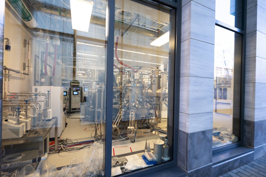
The decision to place the MBE system at MIT.nano was strategic. The facility offers 45,000 square feet of cleanroom space with the infrastructure and expertise necessary to support such a complex instrument.
"MIT.nano's ultra-stable building utilities and lab environment are exactly what is needed to support a system that demands extreme repeatability and purity," says Nick Menounos, MIT.nano associate director of infrastructure. "The success of this installation grew from the early collaboration. Professor Oliver engaged the MIT.nano team in the procurement process almost two years in advance. That foresight, combined with the infrastructure momentum we gained from the recent CHIPS Act project, meant that we could prepare the cleanroom perfectly. We compressed the installation process that normally takes several months and had this extraordinary machine running in under three weeks."
The cleanroom environment is critical for quantum research, where humidity and particle count can significantly affect device performance. By housing the MBE system within MIT.nano, researchers can minimize variables that could impact qubit performance while having access to a comprehensive array of fabrication and metrology tools without leaving the controlled environment.
"We're really excited to see what we can do with it," Strohbeen says. "We bought it as a materials science tool, and it will also be a device development tool due to the flexibility of having it in the cleanroom."
Funding and Future Impact
The MBE system was acquired through a combination of grants from the Army Research Office (ARO) and the Laboratory for Physical Sciences (LPS). The ARO grant, a Defense University Research Instrumentation Program award, specifically targets disruptive technologies in areas of national importance.
This installation arrives at a pivotal moment for MIT's quantum research initiatives. As part of the MIT Quantum Initiative, the system will support efforts to apply quantum breakthroughs to consequential challenges in science, technology, industry, and national security.
"It is a materials scientist's playground," jokes Strohbeen—a controlled space where researchers can explore materials' interactions within layers of atoms, potentially unlocking new pathways toward practical quantum computing systems.
For more information on MIT's quantum research initiatives, visit the Engineering Quantum Systems Group (EQuS) and MIT Quantum Initiative websites.
Comments
Please log in or register to join the discussion