TSMC is developing a glass-based packaging method called Chip-on-Panel-on-Structure, with mass production targeted for late 2028 and Nvidia's Feynman AI chip lined up as the first customer.
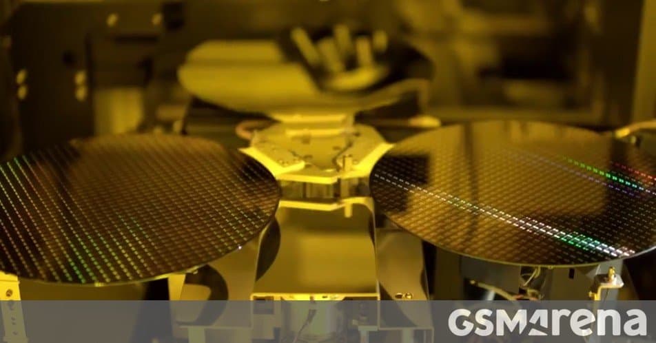
TSMC is working on a new way to package chips, and if the reports hold up, it could reshape how the most demanding processors get built. The technology is called CoPoS, short for Chip-on-Panel-on-Structure, and sources familiar with the work say it relies on a glass material that serves as a temporary carrier before becoming part of a three-layer sandwich substrate in the finished package. Mass production is reportedly slated for the end of 2028.

What CoPoS actually does
To understand why this matters, it helps to separate two parts of chipmaking that often get lumped together. There is the silicon itself, the transistors etched at nodes like 3nm and 2nm, and then there is packaging, the process of mounting that silicon, connecting it to the outside world, and tying multiple chiplets together. For years the conversation focused almost entirely on shrinking transistors. Packaging has quietly become just as important, because modern AI accelerators are no longer single slabs of silicon. They are collections of compute dies, memory stacks, and interconnect glued together into one module.
CoPoS attacks the packaging side. The "panel" in the name is the key idea. Today's advanced packaging largely happens on round silicon wafers, typically 300mm across. A rectangular panel uses area far more efficiently than a circle, which means less wasted substrate per package and more units produced in a single pass. The glass carrier gives the panel a flat, dimensionally stable surface during assembly, then the structure transfers into the final three-layer substrate. The payoff TSMC is reportedly chasing is lower manufacturing cost per package alongside better electrical and thermal performance, which is exactly what large AI chips are starving for.
Why Nvidia gets it first
The first chip expected to use CoPoS is Nvidia's Feynman accelerator, the generation that follows Rubin in Nvidia's data center roadmap. That choice tells you who this technology is for. CoPoS is aimed squarely at AI and high-performance computing, where chips are physically enormous, draw enormous power, and need every bit of bandwidth they can get between compute and high-bandwidth memory. Smartphone and laptop processors are not the priority here, at least not at the start. Those parts are smaller, more cost-sensitive in different ways, and do not push package size to the limits that a training accelerator does.
Packing more silicon and memory into a single package is one of the few levers left for boosting performance now that transistor scaling has slowed and gotten more expensive. A larger, more efficient substrate lets designers place more compute dies and memory stacks side by side without the package falling apart under thermal stress or signal loss. That is the practical reason a packaging breakthrough can matter as much as a new transistor node.
Ecosystem context
This fits a pattern TSMC has been building for a while. The company already sells advanced packaging under the CoWoS and SoIC banners, and demand for those has outstripped supply through the current AI buildout. CoPoS would extend that lead into the next phase. TSMC has publicly forecast the global chip market reaching $1.5 trillion by 2030, driven largely by AI, and its own 2nm chips are expected to cost noticeably more than previous generations. Owning the best packaging gives TSMC leverage that goes beyond just etching transistors.
The competitive angle is real. Samsung and Intel both run foundry businesses and both are investing in their own advanced packaging lines. If CoPoS delivers on cost and performance, rivals will face pressure to ship a credible alternative or cede the most lucrative AI accounts to TSMC. For customers like Nvidia, AMD, and the cloud providers designing their own silicon, the packaging supplier increasingly shapes what their products can do, which is a quieter form of ecosystem lock-in than app stores or operating systems but no less important.
A late 2028 production date means there is plenty of room for the schedule and the details to shift. Panel-level packaging has been discussed across the industry for years precisely because it is hard to get right at scale, with warping and yield on large panels among the recurring challenges. Still, the direction is clear. The race for AI performance is now being run as much in the packaging house as in the lithography fab, and TSMC intends to stay at the front of both. More background on the company's roadmap is available through TSMC's official site.
Comments
Please log in or register to join the discussion