The semiconductor industry faces an unprecedented challenge as 3D IC packages now contain up to 50 million pins, forcing a complete rethink of design methodologies.
The semiconductor industry is undergoing a profound transformation, marked by a critical shift towards 3D IC technology. This evolution is not merely an incremental improvement but a fundamental necessity for the future of electronic systems.
The Pin Count Explosion
We have witnessed package pin counts explode from hundreds of thousands to tens of millions, with projections indicating a potential tenfold increase in the coming years. This overwhelming complexity means that human oversight alone is no longer sufficient.
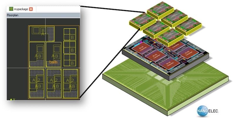
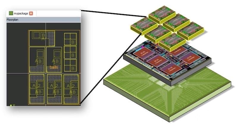
Arrayed blocks are used to construct a chiplet.
The sheer volume of data and the exponential growth in the number of connections within a package have rendered manual synchronization and management of co-designed components an insurmountable challenge.
Traditional Methods Crumble Under Pressure
Traditional approaches to IC packaging design, which often relied on manual methods and generic tools like spreadsheets, are rapidly becoming obsolete in the face of modern complexity. While these tools might have sufficed for simpler, monolithic designs, they are inadequate for the multi-chiplet, multi-interposer assemblies prevalent today.
A single error in a complex package design can lead to costly re-spins, significant delays in product launches, and even complete project failures. The financial implications alone can be devastating, given the immense investment required in semiconductor manufacturing.
Chiplets: Modular Advantage and Integration Challenge
A key enabler in this new era of semiconductor design is the emergence of chiplets. These smaller, standardized building blocks offer a cost-effective alternative to monolithic system-on-chip (SoC) designs, facilitating easier integration and communication through standard interfaces such as UCI Express, BOW, and AIS.
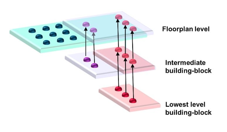
Connectivity in a hierarchical IC package floorplan, showing that bumps within the sub-devices are represented at the top level.
By breaking down large designs into more manageable, reusable components, chiplets promise greater flexibility, faster time-to-market, and improved yield. This modularity allows for the creation of highly customized and optimized systems by combining various specialized chiplets, leading to more efficient and powerful electronic devices.
However, this modularity comes with its own set of challenges, particularly in managing the explosion of interconnections and ensuring seamless integration across multiple disparate dies. The very advantage of chiplets – their ability to enable highly complex, heterogeneous integration – also contributes to the escalating complexity of the overall package.
Hierarchical Device Planning: Abstraction as the Solution
Given the overwhelming complexity now inherent in IC packaging, a fundamental shift towards automated and abstract approaches is essential to break down complexity into manageable portions. The core solution lies in working with abstraction levels, a concept central to hierarchical device planning.
This methodology allows designers to manage the intricate details of chiplet and interposer bump patterns without being overwhelmed by the individual pin-level complexity. While designing viable bump patterns for hundreds of thousands of pins was challenging but feasible in the past, dealing with millions or tens of millions of pins is simply impossible without advanced tools and a hierarchical approach.
Hierarchical device planning enables designers to work at a higher level of abstraction, automating the process of implementing design changes and ensuring consistency across the entire system. This approach not only mitigates the risks associated with manual errors but also significantly improves design efficiency and accelerates the overall development cycle.
A Comprehensive Platform for Next-Generation Design
To navigate the complexities and mitigate the risks inherent in modern IC packaging, designers require sophisticated tools that go far beyond traditional capabilities. These tools must not only manage complexity but also empower designers with insights and automation at every stage of the process.
Addressing these multifaceted challenges, Siemens EDA introduced its Innovator3D IC portfolio solution. This comprehensive suite covers the entire design flow, from initial planning and optimization through detailed analysis, package layout, and crucial work-in-progress (WIP) data management.
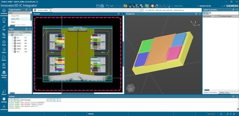
Innovator3D IC solution suite cockpit
The sheer volume of data involved in modern package designs necessitates robust version control and tracking to prevent errors caused by outdated or incorrect files.
The Siemens EDA Innovator3D IC portfolio provides the necessary capabilities to manage the unprecedented scale of integration and pin counts that define the future of chiplet ecosystems, ensuring that designers have the proper methodology and tools for the job.
The Strategic Imperative
The journey through the complexities of modern IC packaging underscores a clear and urgent message: the industry must embrace new methodologies and advanced tools to succeed. While the challenges posed by accelerating complexity, chiplet integration, and exploding pin counts may seem daunting, effective solutions are available.
The future of semiconductor design, characterized by advanced 3D ICs and chiplet integration, demands a proactive approach to adopting sophisticated design automation. By leveraging hierarchical device planning, comprehensive analysis tools, and robust data management solutions like the Siemens EDA Innovator3D IC portfolio, companies can effectively navigate the increasing complexity, mitigate significant risks, and accelerate the development of next-generation electronic systems.
The transition to 3D IC technology is not merely a technological upgrade but a strategic imperative that will shape the future of electronics. By embracing these advancements, the semiconductor industry can unlock new levels of performance, efficiency, and functionality, paving the way for groundbreaking innovations across diverse applications, from artificial intelligence and high-performance computing to automotive and consumer electronics.
Comments
Please log in or register to join the discussion