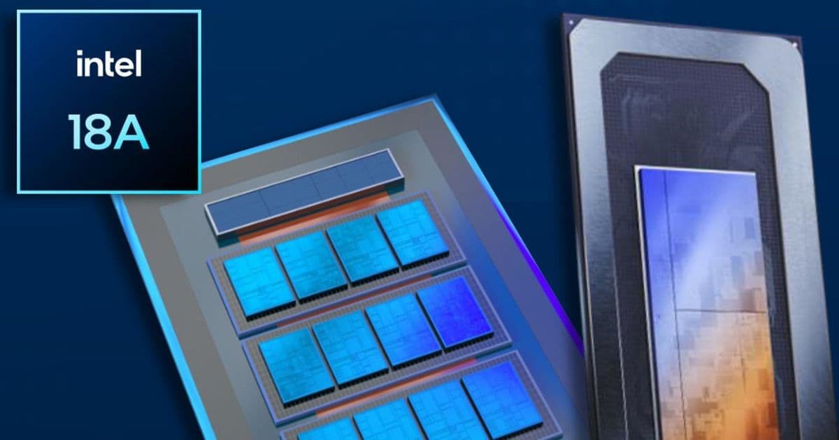
Intel's CFO reveals CEO Lip-Bu Tan has reversed course on 18A, now embracing external foundry business after seeing 'inbound interest' in performance-enhanced 18A-P variant despite ongoing yield challenges.
Intel's 18A fabrication technology, once considered for internal use only, is now attracting external customer interest as the company reports progress on yield improvements and wafer-to-wafer consistency.
From Internal Focus to External Opportunity
When Lip-Bu Tan joined Intel in early 2025, he seriously considered making the company's 18A (1.8nm-class) process an internal-only technology. The decision stemmed from concerns about the node's viability for external foundry customers, particularly given the low and unpredictable yields that plagued the process at the time.
However, speaking at the Morgan Stanley Technology, Media & Telecom Conference 2026, Intel CFO David Zinsner revealed a significant shift in strategy. "While Lip-Bu was, I think, thinking that we probably should focus on 14A as a foundry node and make 18A really just an internal node, now that we have seen some real progress there, I think he is now starting to recognize that this is actually a good node to offer to external customers as well," Zinsner stated.
Growing Interest in 18A-P
The turning point appears to be "inbound interest" in 18A-P, a performance-enhanced variant of the 18A process. This development suggests that potential foundry customers are beginning to see value in Intel's advanced manufacturing capabilities, despite the ongoing challenges.
Zinsner emphasized the positive nature of this interest: "We have been getting some kind of inbound interest in 18A-P as a foundry node. So, I think that is pretty positive."
Yield Challenges Persist
Despite the strategic shift, Intel continues to grapple with process variability issues. The company has made progress on yield improvements, with 18A reaching sufficient maturity to begin low-volume production of Core Ultra 300-series 'Panther Lake' CPU tiles at its Oregon development facility while ramping high-volume manufacturing at Fab 32 in Arizona.
However, wafer-to-wafer parametric variation remains a significant challenge. Zinsner acknowledged the volatility: "There is a lot of volatility, [...] some wafers are yielding a lot less and some are yielding a lot more."
The CFO noted that CEO Tan is particularly focused on minimizing this volatility, and Intel has made "good improvement there." The company expects "a pretty steady yield progression as we go through this year, probably a bit ahead of schedule."
Technical Innovation Meets Manufacturing Reality
Intel's 18A process introduces two groundbreaking technologies: gate-all-around RibbonFET transistors and backside power delivery. These innovations represent significant departures from traditional transistor architectures and power delivery methods, which partly explains the yield challenges.
While such process variability is typical during early high-volume manufacturing ramp-up, it creates capacity unpredictability that complicates supply planning. This unpredictability was likely a key factor in Tan's initial hesitation about promoting 18A externally.
Strategic Implications for Foundry Business
The shift in perspective on 18A has broader implications for Intel's foundry strategy. The company had been considering focusing on 14A (1.4nm-class) for external customers, particularly large clients who make strategic production node decisions years in advance and had opted not to use 18A.
Now, with external interest growing, Intel appears positioned to offer both 18A and 14A as foundry options, potentially appealing to different segments of the market.
Geopolitical Context and Market Opportunities
Recent rumors suggest that several major fabless chip designers have evaluated Intel's 18A and 18A-P process technologies, though none have made public commitments yet. This evaluation phase is crucial as companies assess their manufacturing options in an increasingly complex geopolitical landscape.
Intel's advanced nodes could become particularly attractive to American chip developers looking to increase domestic production capacity. By outsourcing non-core products to Intel, these companies could reduce their geopolitical risks associated with Taiwan and potential tariffs on chips manufactured outside the United States.
The timing is significant, as the semiconductor industry faces increasing pressure to diversify manufacturing locations and reduce dependence on Asian foundries.
Looking Ahead
Intel's journey with 18A illustrates the complex interplay between technical innovation, manufacturing maturity, and market strategy. The company's ability to attract external interest in 18A-P while continuing to improve yields suggests that Intel's advanced process technology may yet become a competitive advantage in the foundry market.
As the semiconductor industry continues to evolve, Intel's success with 18A and its ability to convert evaluation interest into actual production commitments will be closely watched by competitors and customers alike. The company's progress on yield improvement and wafer-to-wafer consistency will be critical factors in determining whether 18A can fulfill its promise as a leading-edge foundry offering.
The coming months will be crucial as Intel works to convert the inbound interest into concrete partnerships and production agreements, potentially reshaping the competitive landscape of advanced semiconductor manufacturing.
Comments
Please log in or register to join the discussion