TSMC plans to mass-produce its N2 node at five fab phases in the technology's first year, an unprecedented parallel ramp backed by roughly $240 billion in capacity spending over the past decade. The foundry expects N2 wafer-out capacity to run 45% ahead of N3B at the same point in its life, with N2/A16 capacity compounding at 70% per year through 2028 and CoWoS and SoIC packaging scaling at 80% and 90% CAGR respectively.
For years the shorthand for TSMC was "the world's largest foundry," a phrase that quietly conceded the broader title of largest advanced-logic producer to Intel. That framing no longer holds. After spending close to $240 billion on capacity over the last ten years, TSMC now operates nine sites with dozens of 300-mm fabs, many of them running EUV-based processes at volumes Intel cannot match. The company's 2025 wafer-processing revenue reached roughly $103.7 billion, about 84% of its $122.4 billion in consolidated sales, with N3 and N5 alone accounting for around 60% of wafer revenue. Intel Foundry, by comparison, booked $17.83 billion, of which only an estimated 10% to 20% came from EUV nodes. On the leading edge, the gap is now measured in multiples, not margins.
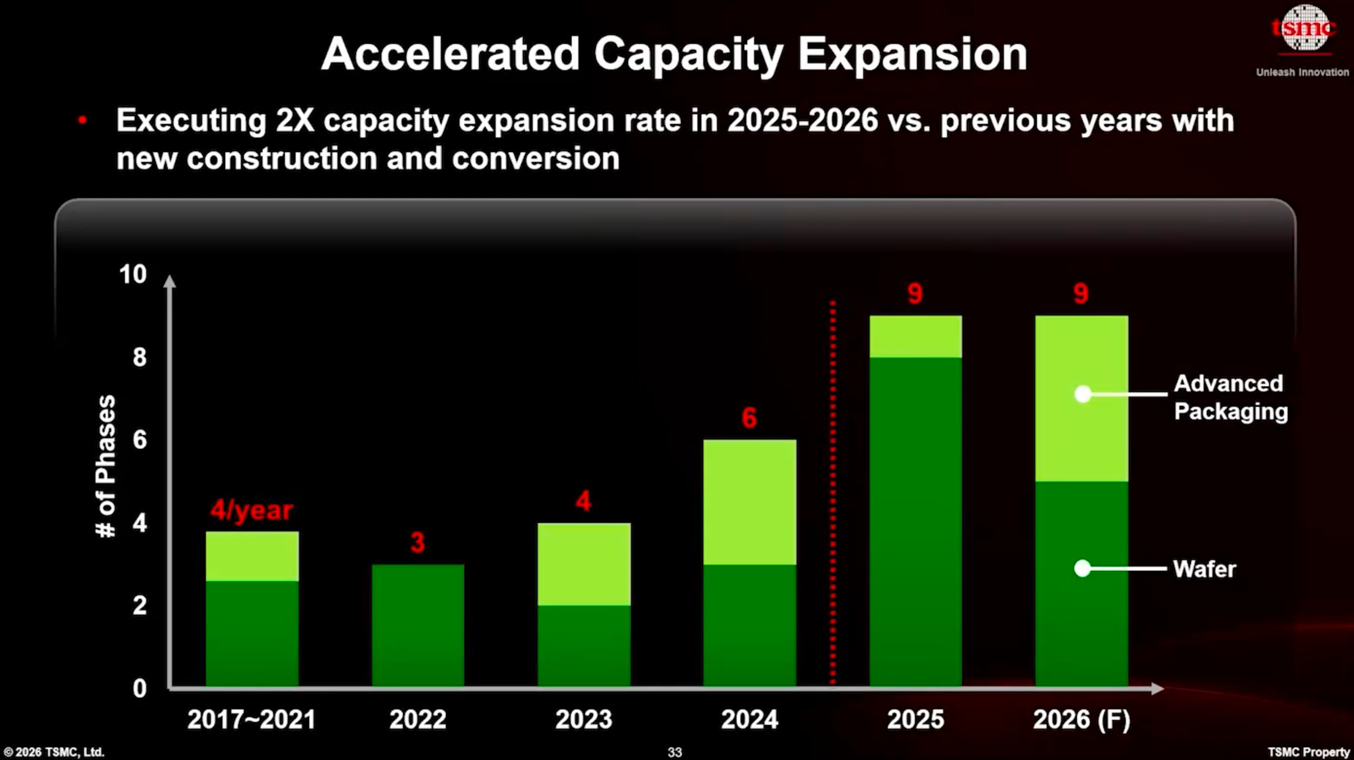
What the company laid out at its Tech Symposium 2026 is less an incremental update than a step change in how fast it can pour concrete and install tools. TSMC effectively doubled its historical construction pace across 2025 and 2026, standing up or converting nine fab phases per year against a long-run average of four. Those phases are spread across Taiwan, Arizona, Japan, and Germany, and they run in parallel rather than in sequence, a scheduling choice that turns out to carry technical advantages beyond simple speed.
The N2 ramp is the centerpiece
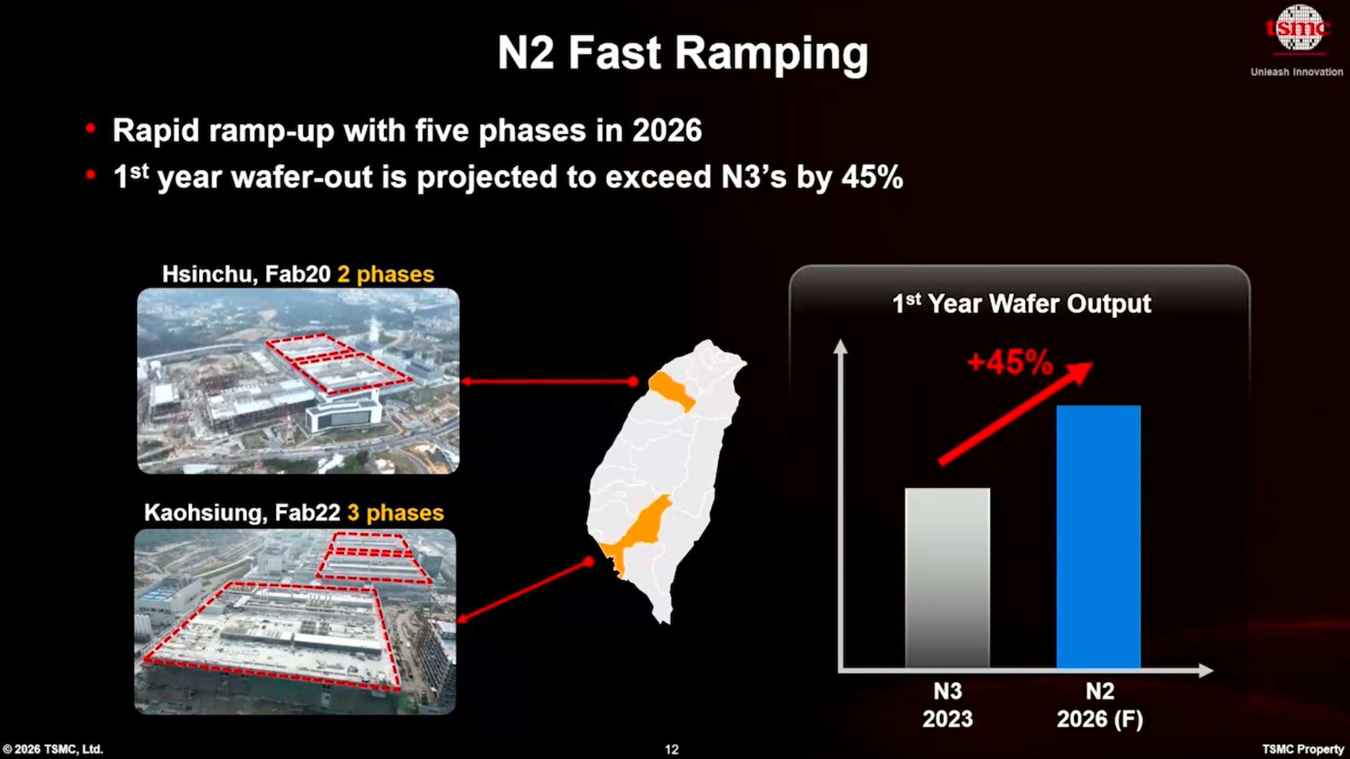
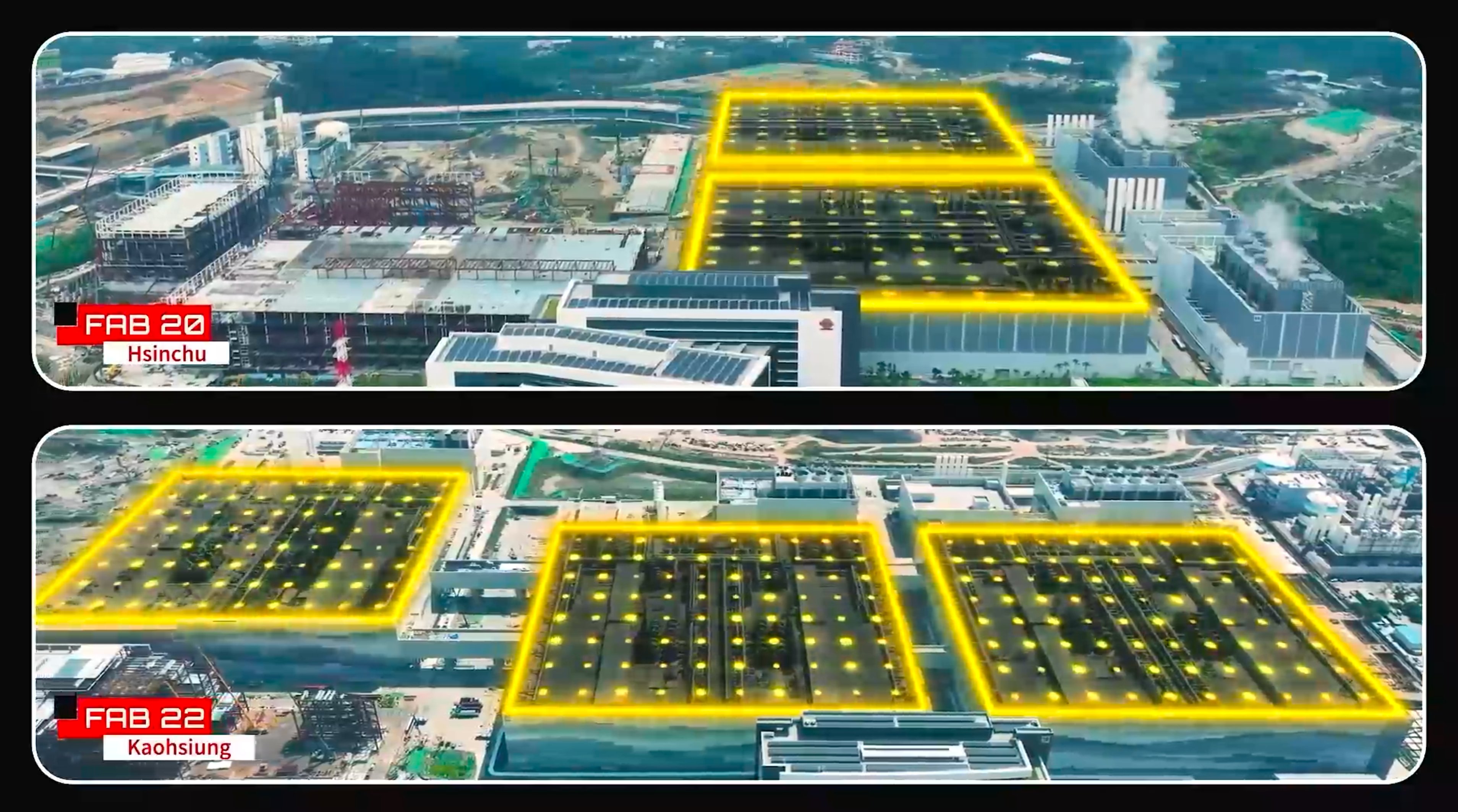
N2, TSMC's first gate-all-around (GAA) nanosheet node, anchors the entire expansion. The company is already ramping it at three locations at once: Fab 20 phases 1 and 2 in Hsinchu, adjacent to its global R&D center, and Fab 22 phase 1 in Kaohsiung. Bringing a leading-edge node up at three sites simultaneously is unusual for any foundry. TSMC intends to push further, ramping Fab 22 phase 2 shortly, phase 3 by year-end, and phase 4 thereafter. The target is mass production across five fab phases inside the node's first year.
The capacity math is the headline. TSMC expects N2 wafer-out volume to run 45% higher than N3B at the equivalent point in its ramp. N3B reached roughly 60,000 wafer starts per month (WSPM) at Fab 18 by the end of 2023, which implies N2 landing near 90,000 WSPM by the end of its first year. For context, Intel's 18A-capable Fab 52 is believed to top out around 40,000 WSPM. From there, TSMC plans to grow N2/A16 capacity by 70% every year through 2028, a trajectory that points to hundreds of thousands of WSPM by 2029.
Parallel ramps also function as risk management. A contamination event, tool failure, or yield excursion at one phase no longer threatens the entire N2 supply. Splitting production between Hsinchu and Kaohsiung adds geographic insurance against an earthquake or utility outage hitting both at once. For customers like Apple, AMD, Nvidia, and Qualcomm, all of whom need uninterrupted supply, that redundancy is not a nicety.
One Team and the Super Manufacturing Platform
A ramp this aggressive only works with the organizational plumbing to support it. TSMC credits two programs: "One Team," a knowledge-transfer structure linking R&D, process integration, equipment management, and high-volume manufacturing, and the Super Manufacturing Platform (SMP), a centralized control system that makes multiple fabs behave as one. The combination invites comparison to Intel's longstanding "Copy Exactly" discipline.
The logic of One Team is to insert manufacturing teams early in node development so R&D adjusts to what fabs can actually build, tightening the feedback loop and letting yield learning transfer quickly from one site to another. TSMC says the approach delivered 20% faster technology transfer versus N3. SMP, now running across all GigaFab sites, standardizes recipes, tool configurations, metrology, and yield-management flows so fixes propagate globally and customer requalification shrinks when production shifts between fabs.
There is a counterintuitive payoff here. Because every fab phase generates its own tool-behavior, defect-density, and process-window data, running several ramps in parallel can accelerate yield learning rather than dilute it, provided SMP and One Team are stitching the data together. That feedback may be part of why TSMC reports N2 tracking a better yield-learning curve than N3 despite the added complexity of nanosheet transistors. A 70% CAGR in leading-edge capacity would be nearly impossible to coordinate across multiple Fab 22 phases, Fab 20, and eventually Fab 21 in Arizona without that scaffolding.
Beyond N2: A16, A14, and the road to A12
N2 and its variants (N2P, N2X, N2U) plus A16, which is essentially N2P with a backside power delivery network, will concentrate at Fab 20 phases 1 and 2 and across Fab 22's four phases, with some spillover to Fab 21 phase 3. For the nodes past 2nm-class, A14, A13, and A12, TSMC is building Fab 21 phase 3 in Arizona and an entirely new site, Fab 25, in central Taiwan with at least four planned phases. A14 is slated for high-volume production in late 2028 and could ramp at both Fab 20 phase 3 and Fab 25 phase 1. How TSMC intends to upgrade existing N2/A16 fabs to later nodes, if it does at all, remains unstated.
The mature and mid-range nodes keep growing too
The buildout is not confined to the bleeding edge. TSMC is growing combined N3 and N5 capacity at a 25% CAGR from 2022 through 2027. To meet near-term demand it is converting some N5 lines to N3, an inexpensive move because N3 reuses 85% to 90% of N5 tooling. With much of both nodes concentrated at Fab 18 in Tainan (four N5 phases, four N3 phases), the conversion is logistically straightforward.
AI now sits inside the manufacturing flow itself, which produces the slightly recursive picture of TSMC using AI to build more AI accelerators. Modern fabs run roughly 5,000 process steps, and batch processing creates idle time as a cassette of 25 wafers waits for a lithography tool to handle them one at a time. Rapidus president Atsuyoshi Koike argues single-wafer processing could compress cycle times at the expense of tool efficiency. TSMC is taking the opposite tack, squeezing more out of existing tools rather than redesigning the flow. The company described intelligent scheduling built on "state-of-the-art linear programming and heuristic algorithms," generative AI tuning that pushes equipment toward its physical limits while holding wafer quality, and big-data log analysis with text mining to trim idle time and time chamber cleaning precisely. AI-assisted tool verification cut qualification time by more than 20%, which directly speeds new-module ramps.
Expansion beyond Taiwan
In Arizona, Fab 21 phase 1 is producing N4 silicon with capacity rising 1.8X this year, while phase 2 is on track for N3 in Q3 2027 and phase 3 targets N2 later this decade. TSMC continues building shells for phases 3 and 4 and reaffirmed plans for an advanced packaging facility, an R&D center, and further land purchases.
In Japan, Kumamoto's Fab 23 phase 1 already makes 28nm and 22nm parts, while phase 2 shifted from its original 7nm plan to processes down to N3 in response to stronger local demand and onshoring by Japanese chip designers. The Dresden site in Germany, still under construction, targets automotive and industrial work with planar and FinFET 28nm, 22nm, N16, and N12 nodes.
Advanced packaging becomes co-equal with the fab
AI demand is reshaping the back end as much as the front. TSMC said AI-accelerator wafer shipments should rise 11X between 2022 and 2026, while shipments of very large dies above 500 mm2 grow 6X over the same span. Those designs consume both wafer starts and advanced packaging, since many pair logic with HBM3E. CoWoS capacity is set to grow at an 80% CAGR from 2022 to 2027, SoIC at 90%, and TSMC has cut development-to-HVM transition times by 30% for CoWoS and 75% for SoIC versus earlier generations.
The company runs 11 advanced packaging sites across Taiwan, and according to a recent DigiTimes report, it is expanding AP5, AP6, AP7, and AP8 in parallel. AP7 in Chiayi is reportedly slated to become its largest SoIC campus, positioned for customers like Nvidia, which plans 3D packaging for its next-generation Feynman GPUs. AP8, converted from a former Innolux LCD fab, is expected to clear 40,000 wafers per month of CoWoS by late 2026. On the SoIC side, AP6 in Zhunan could approach 10,000 wafers per month and AP7B may add roughly 12,000, with later AP7 phases supporting both SoIC and CoPoS, the latter a 2030s roadmap item. All of it depends on a tightly coordinated ecosystem of HBM suppliers, substrate and material vendors, OSAT and test partners, and toolmakers that TSMC increasingly standardizes around.
The full picture

The roadmap reads as a single coordinated bet. TSMC has doubled its construction cadence, is ramping N2 at five phases in year one, and projects 70% annual growth in leading-edge capacity through 2028, all synchronized through One Team and SMP and accelerated by AI-driven fab optimization. Advanced packaging scales alongside at 80% to 90% CAGR. Each piece reinforces the others: more wafer capacity needs more packaging, parallel ramps feed faster yield learning, and standardized control lets the whole network move as one. For Intel and Samsung Foundry, the challenge is no longer matching a single node. It is matching the rate at which a competitor can build, fill, and synchronize fabs across four countries at once. You can read the full breakdown at Tom's Hardware and TSMC's own technology overview.
Comments
Please log in or register to join the discussion